


|
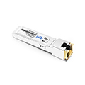
产品型号
|
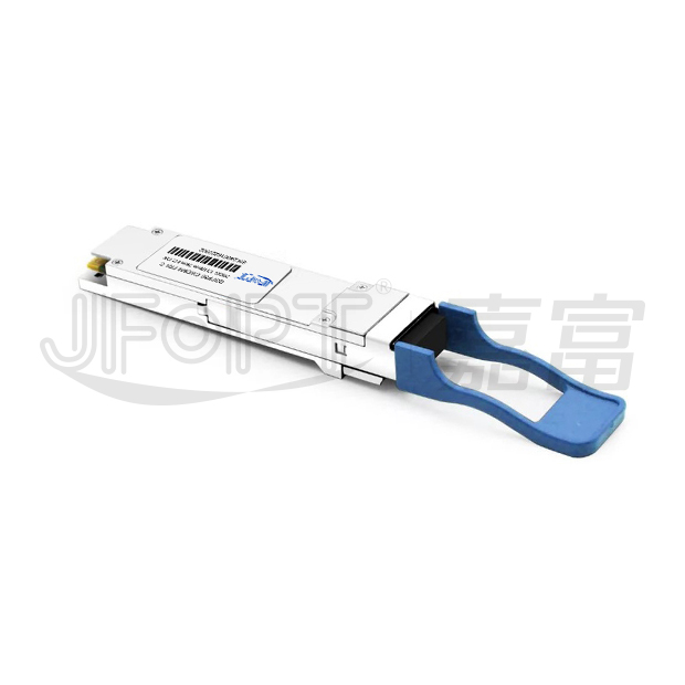
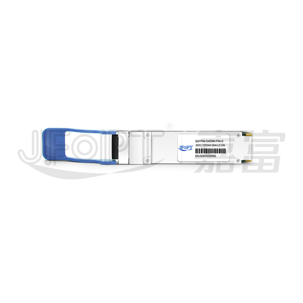
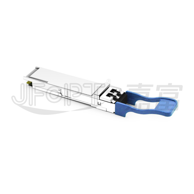
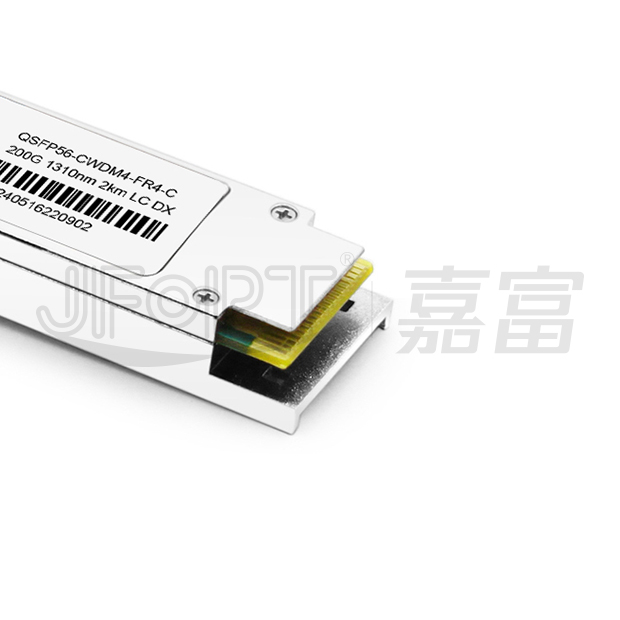
JFTSM-QSFP56-200(4x50)-CW4-2(FR4)-LCD
|
工厂品牌
|
JFOPT嘉富
|
|
封装形式
|
QSFP56
|
光口类型
|
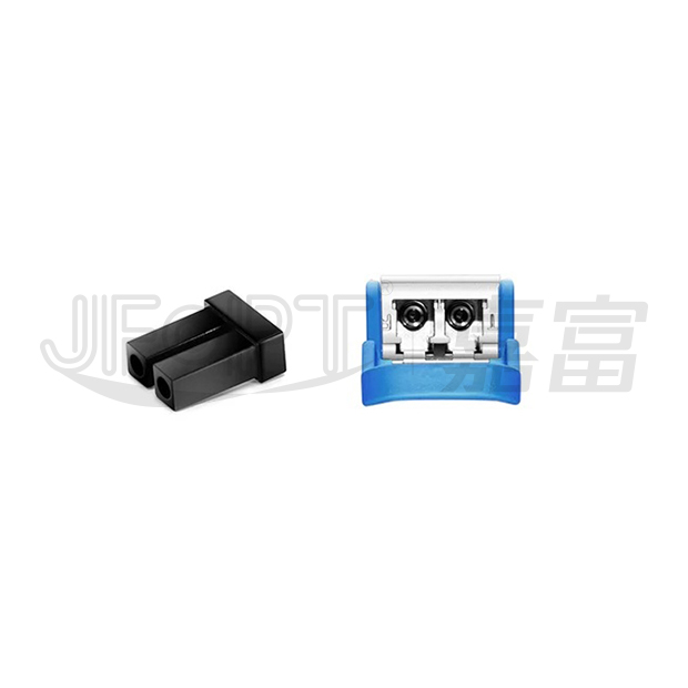
LC双联
|
|
最高总速率
|
200Gbps
|
每通道速率
|
26.5625Gbps
|
|
最大传输距离
|
2km
|
||
|
工作波长
|
1310nm
|
工作电压
|
3.3V
|
|
光纤型号
|
SMF
|
纤芯尺寸
|
9/125
|
|
发射器类型
|
CWDM LD&PD
|
接收器类型
|
PIN
|
|
发射功率
|
-4.2~4.7dBm
|
接收灵敏度
|
-6dBm
|
|
数字诊断(DDM)
|
YES
|
接收过载
|
4.7dBm
|
|
功耗
|
<6.5W
|
支持协议
|
200G BASE-FR4 ethernet
Switch & Router Connections Data center Other 200G interconnect requirements |
|
工作温度(商业级)
|
0℃~+70℃
|
储存温度(商业级)
|
-40℃~+85℃
|
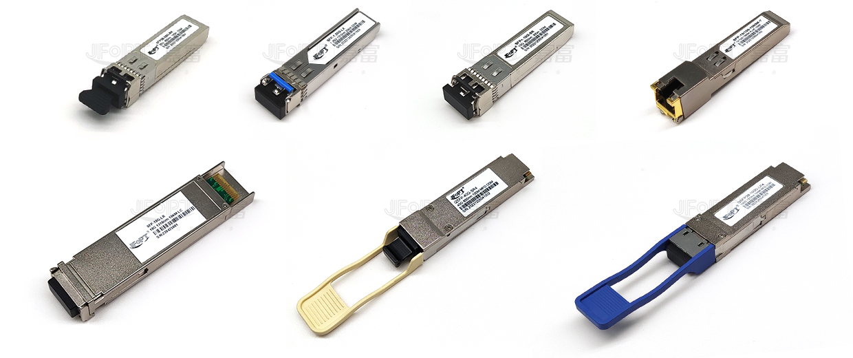
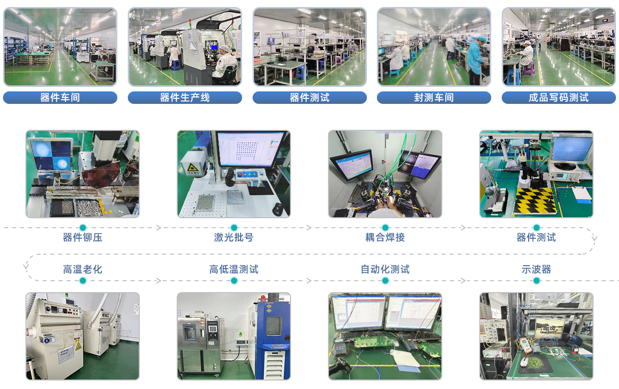
JFOPT嘉富持续投入光模块生产领域,产品覆盖1*9、SFP、10G、25G、100G、200G、400G、800G GPON/EPON/XG/XGSPON OLT等全系列光模块。同时为下游同行提供TOSA、ROSA、BOSA等光器件半成品解决方案。JFOPT嘉富生产线具备日产量一万只光模块、两万只光器件的能力。此外,JFOPT嘉富光模块拥有业界领先的耐高温、抗干扰特性,广泛应用于计算中心、运营商、交通安防、电力设施等行业领域。
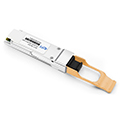
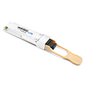
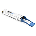
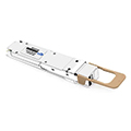
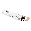
JFOPT QSFP56 200G (4x50G) CWDM4 2km FR4 LC DX光模块是一款高性能热插拔模块,采用PAM4调制技术实现每通道50Gbps的光数据传输。该模块支持通过单模光纤进行最长2公里的数据传输,采用紧凑型QSFP56封装。其内部集成先进组件,包括高性能激光二极管(LD)、光电探测器(PIN)和数字信号处理器(DSP),可确保在严苛的数据通信应用场景中实现稳定高效的运行。
| Hot-pluggable QSFP56 form factor | LC/UPC connecting interface compliant | ||||||||
| Data rate up to 50 Gb/s PAM4 per lane | Integrated CWDM LD and PD array | ||||||||
| Maximum link length of 2km via SMF fiber | Digital diagnostics functions are available via the I2C interface | ||||||||
| Single 3.3V power supply | Power dissipation:<6.5W | ||||||||
| International class 1 laser safety certified | Operating case temperature:0℃~+70℃ |
| 200G BASE-FR4 ethernet | Switch & Router connections | |||||||
| Data centers | Other 200G interconnect requirements | |||||||
| Parameter | Symbol | Min. | Max. | Unit | |||||
| Power supply voltage | VCC | -0.5 | +3.6 | V | |||||
| Storage temperature | TC | -40 | +85 | ℃ | |||||
| Relative humidity | RH | 5 | 85 | % | |||||
These values represent the damage threshold of the module.Stress in excess of any of the individual absolute maximum ratingscan cause immediate catastrophic damage to the module even if all other parameters are within recommended operating conditions.
| Parameter | Symbol | Min | Typical | Max | Unit | ||||
| Power supply voltage | VCC | 3.135 | 3.30 | 3.465 | V | ||||
| Operating case temperature | Tca | 0 | - | 70 | ℃ | ||||
Recommended operating environment specifies parameters for which the electrical and optical characteristics hold unless otherwise noted.
| Parameter | Symbol | Min | Typical | Max | Unit | Notes | |||
| Signaling rate per lane | - | - | 26.5625 | - | Gbd | - | |||
Transmitter |
|||||||||
| Differential data input voltage | △Vin | 900 | - | - | mVp-p | - | |||
| DifferentialInput Impedance | Zin | 90 | 100 | 110 | ohm | - | |||
Receiver |
|||||||||
| Differential output voltage | Vout | - | - | 900 | mVp-p | - | |||
| Differential output impedance | Rout | 90 | 100 | 110 | ohm | - | |||
| Parameter | Symbol | Min | Typical | Max | Unit | Notes | |||
Transmitter |
|||||||||
| Center wavelength | Ch0 | λ0 | 1264.5 | 1271 | 1277.5 | nm | - | ||
| Ch1 | λ1 | 1284.5 | 1291 | 1297.5 | |||||
| Ch2 | λ2 | 1304.5 | 1311 | 1317.5 | |||||
| Ch3 | λ3 | 1324.5 | 1331 | 1337.5 | |||||
| Side-mode suppression ratio | SMSR | 30 | - | - | dB | - | |||
| Average optical power | Po | -4.2 | - | 4.7 | dBm | - | |||
| Tx OMA per lane | TxOMA | -1.2 | - | 4.5 | dBm | - | |||
| Extinction ratio | ER | 3.5 | - | - | dBm | - | |||
| Optical modulation amplitude | OMA | -4.5 | - | 3 | dB | - | |||
| Transmitter and dispersion eye closure for PAM4 per lane | TDECQ | - | - | 3.3 | dB | - | |||
| Optical return loss tolerance | ORL | - | - | 16.5 | dB | - | |||
| Relative intensity noise | RIN | - | - | -132 | dB/Hz | - | |||
Receiver |
|||||||||
| Center wavelength | Ch0 | λ0 | 1264.5 | 1271 | 1277.5 | nm | |||
| Ch1 | λ1 | 1284.5 | 1291 | 1297.5 | |||||
| Ch2 | λ2 | 1304.5 | 1311 | 1317.5 | |||||
| Ch3 | λ3 | 1324.5 | 1331 | 1337.5 | |||||
| Damage threshold | DT | 5.7 | - | - | dBm | - | |||
| Average receive power ,each lane | - | -8.2 | - | 4.7 | dBm | - | |||
| Receiver reflectance | Rfl | - | - | -26 | dB | - | |||
| Difference in receive power between any two lanes | - | - | - | 4.1 | dB | - | |||
| Receiver sensitivity(OMAouter) | - | - | - | -6 | dBm | - | |||
| Stressed receiver sensitivity(OMAouter) | - | - | - | -3.6 | dBm | - | |||
The following optical characteristics are defined over the recommended operating environment unless otherwise specified.
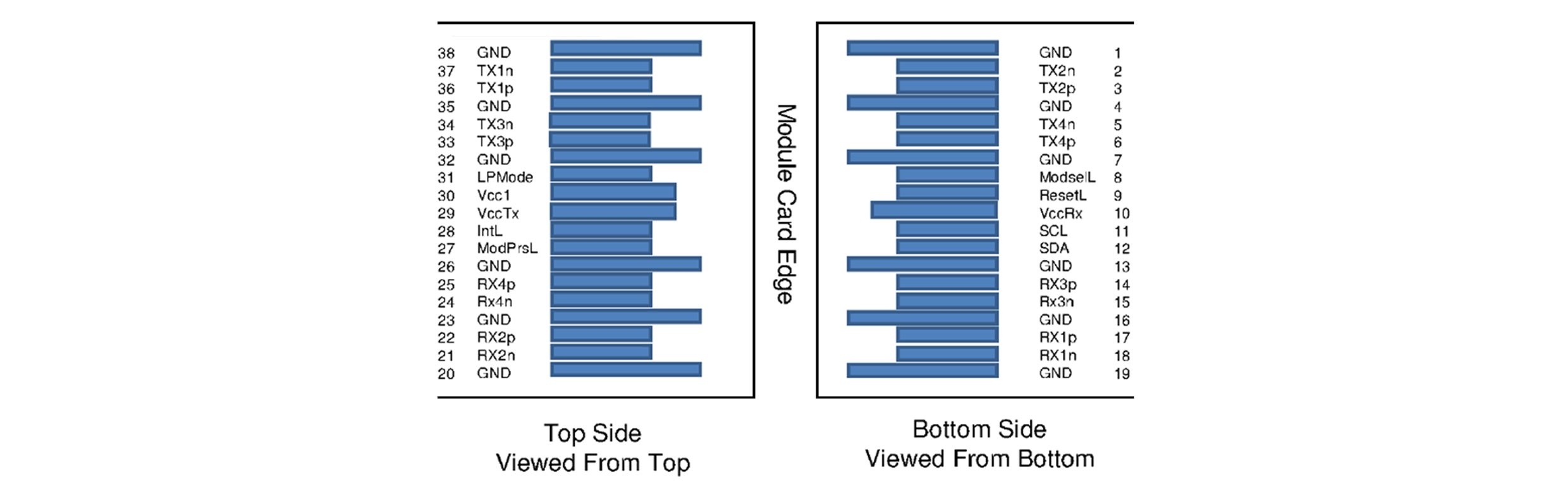
| Pin | Symbol | Name/Description | |||||||
| 1 | GND | Ground | |||||||
| 2 | Tx2n | Transmitter inverted data input | |||||||
| 3 | Tx2p | Transmitter non-inverted data input | |||||||
| 4 | GND | Ground | |||||||
| 5 | Tx4n | Transmitter inverted data input | |||||||
| 6 | Tx4p | Transmitter non-inverted data input | |||||||
| 7 | GND | Ground | |||||||
| 8 | ModSelL | Module select | |||||||
| 9 | ResetL | Module reset | |||||||
| 10 | VCCRx | +3.3V power supply receiver | |||||||
| 11 | SCL | 2-wire serial interface clock | |||||||
| 12 | SDA | 2-wire serial interface data | |||||||
| 13 | GND | Ground | |||||||
| 14 | Rx3p | Receiver non-inverted data output | |||||||
| 15 | Rx3n | Receiver inverted data output | |||||||
| 16 | GND | Ground | |||||||
| 17 | Rxlp | Receiver non-inverted data output | |||||||
| 18 | Rx1n | Receiver inverted data output | |||||||
| 19 | GND | Ground | |||||||
| 20 | GND | Ground | |||||||
| 21 | Rx2n | Receiver inverted data output | |||||||
| 22 | Rx2p | Receiver non-inverted data output | |||||||
| 23 | GND | Ground | |||||||
| 24 | Rx4n | Receiver inverted data output | |||||||
| 25 | Rx4p | Receiver non-inverted data output | |||||||
| 26 | GND | Ground | |||||||
| 27 | ModPrsL | Module present | |||||||
| 28 | IntL | Interrupt | |||||||
| 29 | VCC Tx | +3.3V power supply transmitter | |||||||
| 30 | VCC1 | +3.3V power Supply | |||||||
| 31 | LPMode | Low power mode | |||||||
| 32 | GND | Ground | |||||||
| 33 | Tx3p | Transmitter non-inverted data input | |||||||
| 34 | Tx3n | Transmitter inverted data input | |||||||
| 35 | GND | Ground | |||||||
| 36 | Txlp | Transmitter non-inverted dataInput | |||||||
| 37 | Tx1n | Transmitter inverted data input | |||||||
| 38 | GND | Ground | |||||||


 Wendy
Wendy Sophie
 Jeanne


