


|
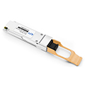
产品型号
|
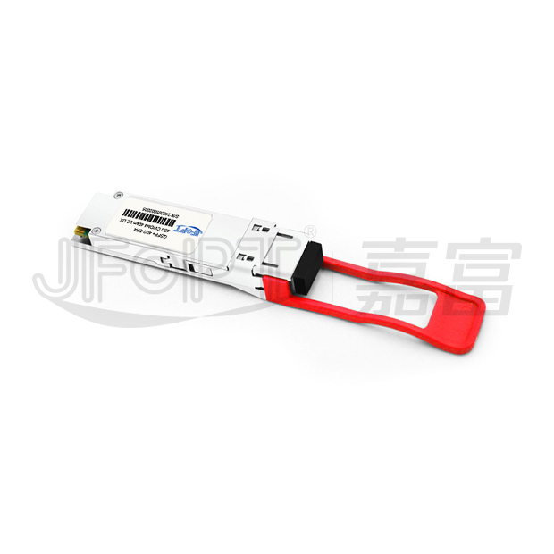
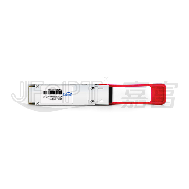
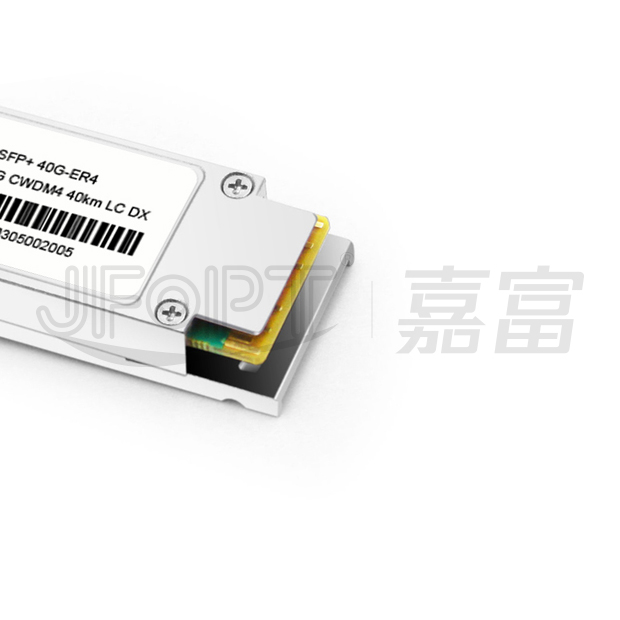
JFTSM-QSFP+40-CW4-40(ER4)-LCD
|
工厂品牌
|
JFOPT
|
|
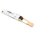
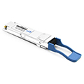
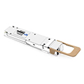
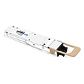
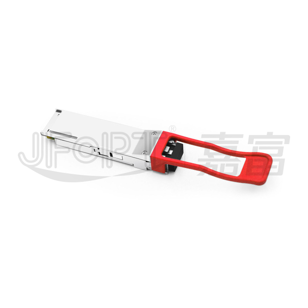
封装形式
|
QSFP+
|
光口类型
|
LC 双联
|
|
最高总速率
|
40Gbps
|
每通道速率
|
10.3125Gbps
|
|
最大传输距离
|
40km
|
||
|
工作波长
|
1271nm, 1291nm
1311nm, 1331nm
|
工作电压
|
3.3V
|
|
光纤型号
|
SMF
|
纤芯尺寸
|
9/125
|
|
发射器类型
|
DFB CWDM
|
接收器类型
|
APD
|
|
发射功率
|
-2.7~4.5dBm
|
接收灵敏度
|
<-21.2dBm
|
|
数字诊断
|
YES
|
接收过载
|
-4.5dBm
|
|
功耗
|
Commercial≤3.5W
Industrial≤4.5W
|
支持协议
|
IEEE 802.3ba 40GBASE-ER4
|
|
工作温度(商业级)
|
0℃~+70℃
|
储存温度(商业级)
|
-40℃~+85℃
|
|
工作温度(工业级)
|
-40℃~+85℃
|
储存温度(工业级)
|
-40℃~+85℃
|
生产线介绍
PRODUCTION LINE INTRODUCTION
JFOPT嘉富持续投入光模块生产领域,产品覆盖1*9、SFP、10G、25G、100G、200G、400G、800G GPON/EPON/XG/XGSPON OLT等全系列光模块。同时为下游同行提供TOSA、ROSA、BOSA等光器件半成品解决方案。JFOPT嘉富生产线具备日产量一万只光模块、两万只光器件的能力。此外,JFOPT嘉富光模块拥有业界领先的耐高温、抗干扰特性,广泛应用于计算中心、运营商、交通安防、电力设施等行业领域。
产品介绍
PRODUCT PRESENTATION
JFOPT QSFP+ 40G CWDM4 40km ER4 LC DX光模块专为40GbE单模光纤(SMF)连接设计,传输距离可达40公里。该模块符合IEEE 802.3ba 40GBASE-ER4标准,并通过QSFP+ MSA规定的I2C接口提供数字诊断功能。
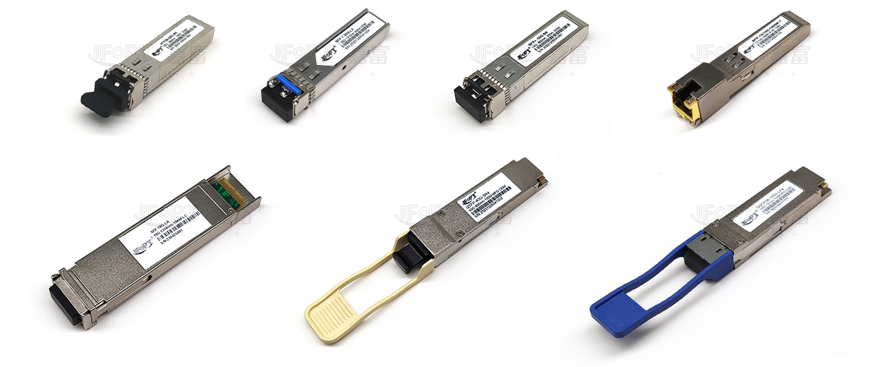
光模块系列产品
TRANSCEIVER SERIES PRODUCTS
生产及检测设备
PRODUCTION & TESTING EQUIPMENT
产品特点
FEATURES
| Supports 40Gbps | Single 3.3V power supply | ||||||||
| Commercial power dissipation <3.5W and and industrial power dissipation <4.5W | Up to 40km over SMF | ||||||||
|
Operating case temperature range of
Standard: 0°C to 70°C
Industrial: -40°C to 85°C
|
Four 10G DFB base CWDM channels on transmitter side | ||||||||
| Duplex LC receptacles | I2C interface with integrated digital diagnostic monitoring | ||||||||
| Safety certification: TUV/UL/FDA | RoHS compliant |
应用范围
APPLICATION
符合标准
STANDARD COMPLIANCE
绝对最大额定值
ABSOLUTE MAXIMUM RATINGS
| Parameter | Symbol | Min. | Max. | Unit | ||||
| Storage temperature | TS | -40 | +85 | °C | ||||
| Supply voltage | VCC | -0.5 | 3.6 | V | ||||
| Operating relative humidity | RH | 0 | 85 | % | ||||
*Exceeding any one of these values may destroy the device immediately.
建议操作条件
RECOMMENDED OPERATING CONDITIONS
| Parameter | Symbol | Min. | Typical | Max. | Unit | |||
| Operating case temperature | Tc | JFTSM-QSFP+40-CW4-40(ER4)-LCD | 0 | - | +70 | °C | ||
| -40 | - | +85 | °C | |||||
| Power supply voltage | Vcc | 3.135 | 3.3 | 3.465 | V | |||
| Commercial power dissipation | PD | - | - | 3.5 | W | |||
| Industrial power dissipation | PD | - | - | 4.5 | W | |||
| Link distance with G.652 | D | - | - | 40 | km | |||
性能规范-电气
PERFORMANCE SPECIFICATIONS - ELECTRICAL
| Parameter | Symbol | Min. | Typ. | Max | Unit | Notes | ||
| Supply voltage | - | 3.1 | - | 3.47 | V | - | ||
| Supply current | Icc | - | - | 1.44 | A | - | ||
| Transmit turn-on time | - | - | - | 2000 | ms | Note3 | ||
Transmitter |
||||||||
| Differential input voltage swing |
Vin,pp | 190 | - | 700 | mVp-p | - | ||
| Input impedance (Differential) | Zin | 90 | 100 | 110 | ohms | Rin > 100 kohms @ DC |
||
Receiver |
||||||||
| Differential output voltage swing |
Vout,pp | 300 | - | 850 | mVp-p | - | ||
| AC common mode output voltage |
- | - | - | 7.5 | mV | RMS | ||
| Output impedance (Differential) |
Zout | 90 | 100 | 110 | ohms | - | ||
| Output transition time | - | 28 | - | - | ps | 20%~80% | ||
40GBASE-ER4 操作
40GBASE-ER4 OPERATION
| Parameter |
Symbol
|
Min. | Typical | Max. | Unit | |||
Transmitter |
||||||||
| Signaling speed per lane | BRAVE | - | 10.3125 | 11.2 | Gbps | |||
| Side mode launch power | SMSR | 30 | - | - | dB | |||
| Total average launch power | PT | - | - | 10.5 | dBm | |||
| Lane_0 center wavelength | λC0 | 1264.5 | 1271 | 1277.5 | nm | |||
| Lane_1 center wavelength | λC1 |
1284.5
|
1291 | 1297.5 | nm | |||
| Lane_2 center wavelength | λC2 | 1304.5 | 1311 | 1317.5 | nm | |||
| Lane_3 center wavelength | λC3 | 1324.5 | 1331 | 1337.5 | nm | |||
| Average launch power per lane | Peach | -2.7 | - | 4.5 | dBm | |||
| Average launch power of OFF transmitter per lane | - | - | - | -30 | dBm | |||
| Relative intensity noise | Rin | - | - | -128 | dB/Hz | |||
| Optical modulation amplitude | Poma | 0.3 | 0 | 5.0 | dBm | |||
| Optical return loss tolerance | - | - | - | 20 | dB | |||
| Differnce in launch power between any two lanes | Ptx,diff | - | - | 4.7 | dB | |||
| Transmitter reflectance | RT | - | - | -12 | dB | |||
| Extinction ratio | ER | 5.5 | - | - | dB | |||
| Transmitter eye mask definition{X1, X2, X3, Y1, Y2, Y3} | - | {0.25 ,0.4 ,0.45 ,0.25 ,0.28 ,0.4} | - | |||||
Receiver |
||||||||
| Signaling speed per lane | BRAVE | - | 10.3125 | - | Gbps | |||
| Data rate variation | -100 | - | +100 | ppm | ||||
| Damage threshold | Rdam | 3.8 | - | - | dBm | |||
| Lane_0 center wavelength | λC0 | 1264.5 | 1271 | 1277.5 | nm | |||
| Lane_1 center wavelength | λC1 | 1284.5 | 1291 | 1297.5 | nm | |||
| Lane_2 center wavelength | λC2 | 1304.5 | 1311 | 1317.5 | nm | |||
| Lane_3 center wavelength | λC3 | 1324.5 | 1331 | 1337.5 | nm | |||
| Average receive power per lane | Rpow | -21.2 | - | -4.5 | dBm | |||
| Receiver sensitivity in OMA per lane | Pmin | - | - | -19 | dBm | |||
| Stressed receiver sensitivity (OMA) per lane | RXSRS | - | - | -16.8 | dBm | |||
Conditions of stressed receiver sensitivity test: |
||||||||
| Vertical eye closure penalty | VECP | - | 2.2 | - | dB | |||
| Stressed J2 jitter | J2 | - | 0.3 | - | UI | |||
| Stressed J9 jitter | J9 | - | 0.47 | - | UI | |||
| LOS assert | LOSA | -35 | - | - | dBm | |||
| LOS de-assert | LOSD | - | - | -23 | dBm | |||
| LOS hysteresis | - | 0.5 | - | - | dB | |||
QSFP+收发器电气焊盘布局
QSFP+ TRANSCEIVER ELECTRICAL PAD LAYOUT
引脚排列和定义
PIN ARRANGEMENT AND DEFINITION
| Pin | Logic | Symbol | Description | Plug Sequence | Notes | |||
| 1 | - | GND | Ground | 1 | 1 | |||
| 2 | CML-I | Tx2n | Transmitter Inverted Data Input | 3 | - | |||
| 3 | CML-I | Tx2p | Transmitter Non-Inverted Data Input | 3 | - | |||
| 4 | - | GND | Ground | 1 | 1 | |||
| 5 | CML-I | Tx4n | Transmitter Inverted Data Input | 3 | - | |||
| 6 | CML-I | Tx4p | Transmitter Non-Inverted Data Input | 3 | - | |||
| 7 | - | GND | Ground | 1 | 1 | |||
| 8 | LVTTL-I | ModSelL | Module Select | 3 | - | |||
| 9 | LVTTL-I | ResetL |
Module Reset
|
3 | - | |||
| 10 | - | VccRx | +3.3V Power Supply Receiver | 2 | 2 | |||
| 11 | LVCMOS- I/O | SCL | 2-wire Serial Interface Clock | 3 | - | |||
| 12 | LVCMOS- I/O | SDA | 2-wire Serial Interface Data | 3 | - | |||
| 13 | - | GND | Ground | 1 | 1 | |||
| 14 | CML-O | Rx3p | Receiver Non-Inverted Data Output | 3 | - | |||
| 15 | CML-O | Rx3n | Receiver Inverted Data Output | 3 | - | |||
| 16 | - | GND | Ground | 1 | 1 | |||
| 17 | CML-O | Rx1p | Receiver Non-Inverted Data Output | 3 | - | |||
| 18 | CML-O | Rx1n | Receiver Inverted Data Output | 3 | - | |||
| 19 | - | GND | Ground | 1 | 1 | |||
| 20 | - | GND | Ground | 1 | 1 | |||
| 21 | CML-O | Rx2n | Receiver Inverted Data Output | 3 | - | |||
| 22 | CML-O | Rx2p | Receiver Non-Inverted Data Output | 3 | - | |||
| 23 | - | GND | Ground | 1 | 1 | |||
| 24 | CML-O | Rx4n | Receiver Inverted Data Output | 3 | - | |||
| 25 | CML-O | Rx4p | Receiver Non-Inverted Data Output | 3 | - | |||
| 26 | - | GND | Ground | 1 | 1 | |||
| 27 | LVTTL-O | ModPrsL | Module Present | 3 | - | |||
| 28 | LVTTL-O | IntL | Interrupt | 3 | - | |||
| 29 | - | VccTx | +3.3V Power supply transmitter | 2 | 2 | |||
| 30 | - | Vcc1 | +3.3V Power supply | 2 | 2 | |||
| 31 | LVTTL-I | LPMode | Low Power Mode | 3 | - | |||
| 32 | - | GND | Ground | 1 | 1 | |||
| 33 | CML-I | Tx3p | Transmitter Non-Inverted Data Input | 3 | - | |||
| 34 | CML-I | Tx3n | Transmitter Inverted Data Input | 3 | - | |||
| 35 | - | GND | Ground | 1 | 1 | |||
| 36 | CML-I | Tx1p | Transmitter Non-Inverted Data Input | 3 | - | |||
| 37 | CML-I | Tx1n | Transmitter Inverted Data Input | 3 | - | |||
| 38 | - | GND | Ground | 1 | 1 | |||
1: GND is the symbol for signal and supply (power) common for the QSFP+ module. All are common within the QSFP+ module and all module voltages are referenced to this potential unless otherwise noted. Connect these directly to the host board signal-common ground plane.
2: Vcc Rx, Vcc1 and Vcc Tx are the receiver and transmitter power supplies and shall be applied concurrently. Requirements defined for the host side of the Host Edge Card Connector are listed in Table 6. Recommended host board power supply filtering is shown in Figures 3 and 4. Vcc Rx Vcc1 and Vcc Tx may be internally connected within the QSFP+ Module in any combination. The connector pins are each rated for a maximum current of 500mA.
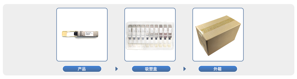
产品包装
PRODUCT PACKAGING
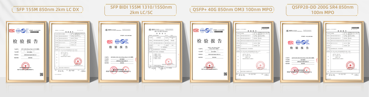
产品认证
PRODUCT CERTIFICATION
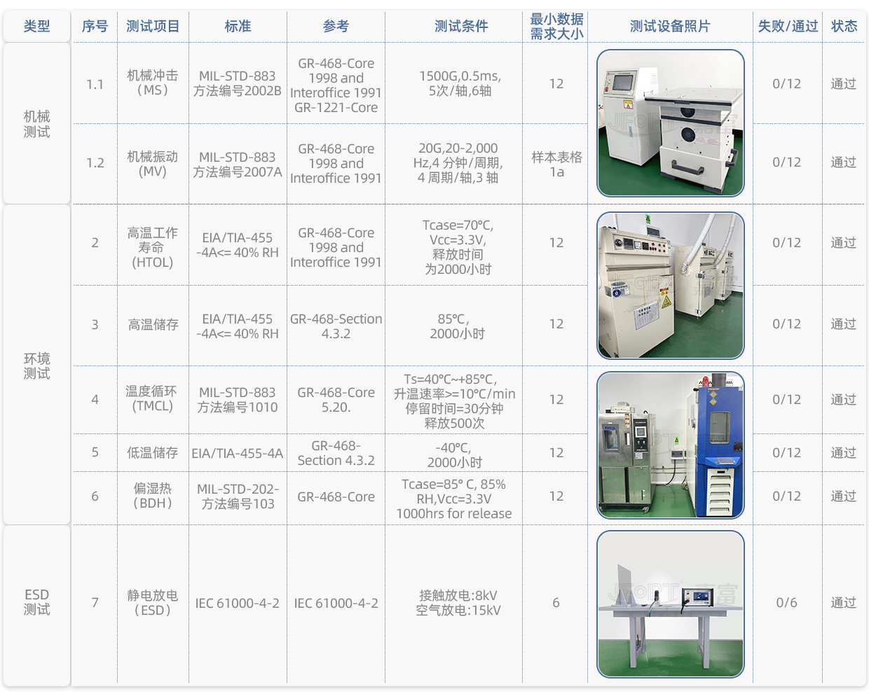
质量优势
QUALITY ADVANTAGE
兼容品牌
COMPATIBLE BRANDS


 Wendy
Wendy Sophie
 Jeanne


