


|
产品型号
|
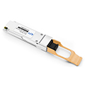
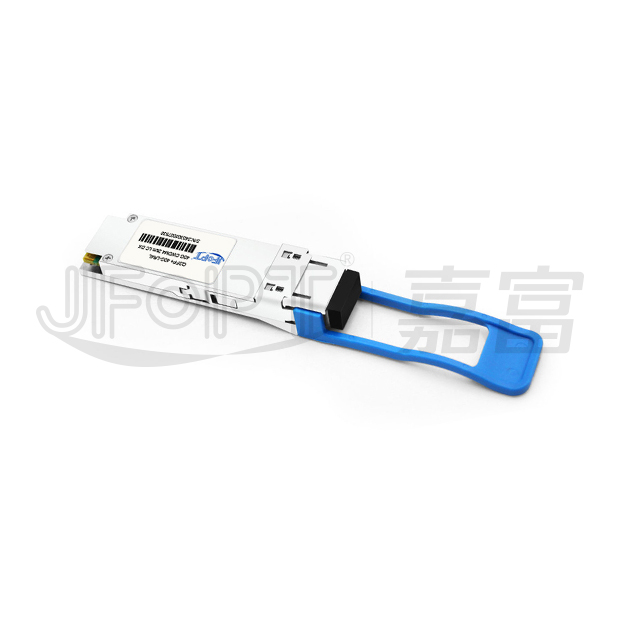
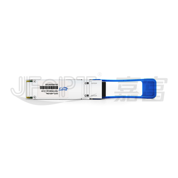
JFTSM-QSFP+40-CW4-2(LR4L)-LCD
|
工厂品牌
|
JFOPT嘉富
|
|
封装形式
|
QSFP+
|
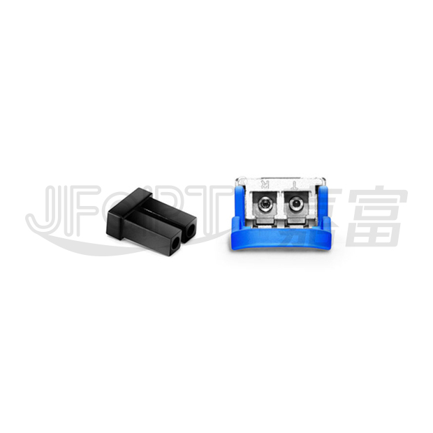
光口类型
|
LC 双联
|
|
最高总速率
|
40G
|
每通道速率
|
11.2Gbps
|
|
最大传输距离
|
2km
|
||
|
工作波长
|
1271nm, 1291nm
1311nm, 1331nm
|
工作电压
|
3.3V
|
|
光纤型号
|
SMF
|
纤芯尺寸
|
9/125
|
|
发射器类型
|
4 Lanes CWDM DFB
|
接收器类型
|
PIN
|
|
发射功率
|
-7.6~+2.3dBm
|
接收灵敏度
|
<-12dBm
|
|
数字诊断(DDM)
|
YES
|
接收过载
|
2.3dBm
|
|
功耗
|
< 3.5W
|
支持协议
|
IEEE802.3ba
40GBASE-IR4 Standard
|
|
工作温度(商业级)
|
0℃~+70℃
|
储存温度(商业级)
|
-40℃~+85℃
|
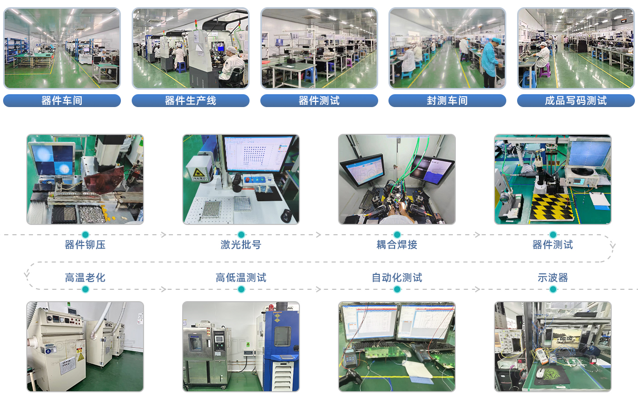
生产线介绍
PRODUCTION LINE INTRODUCTION
JFOPT嘉富持续投入光模块生产领域,产品覆盖1*9、SFP、10G、25G、100G、200G、400G、800G GPON/EPON/XG/XGSPON OLT等全系列光模块。同时为下游同行提供TOSA、ROSA、BOSA等光器件半成品解决方案。JFOPT嘉富生产线具备日产量一万只光模块、两万只光器件的能力。此外,JFOPT嘉富光模块拥有业界领先的耐高温、抗干扰特性,广泛应用于计算中心、运营商、交通安防、电力设施等行业领域。
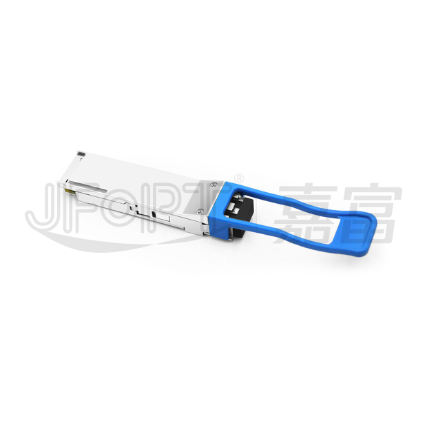
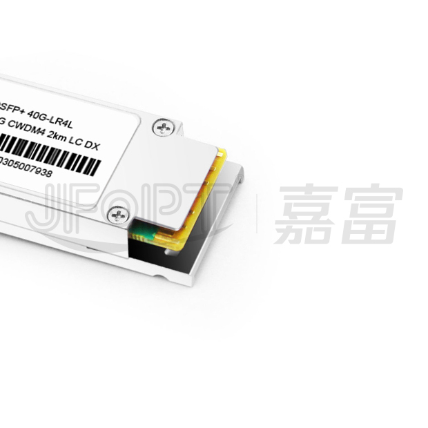
产品介绍
PRODUCT PRESENTATION
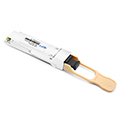
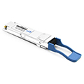
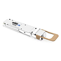
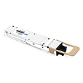
JFOPT QSFP+ 40G CWDM4 2公里 LR4L LC DX光模块专为单模光纤40千兆位链路设计,符合QSFP+ MSA及IEEE 802.3ba 40GBASE-LR4标准。该模块支持通过I2C接口实现数字诊断功能(遵循QSFP+ MSA规范),同时满足欧盟RoHS指令2011/65/EU的环保安全要求。
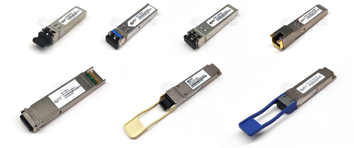
光模块系列产品
TRANSCEIVER SERIES PRODUCTS
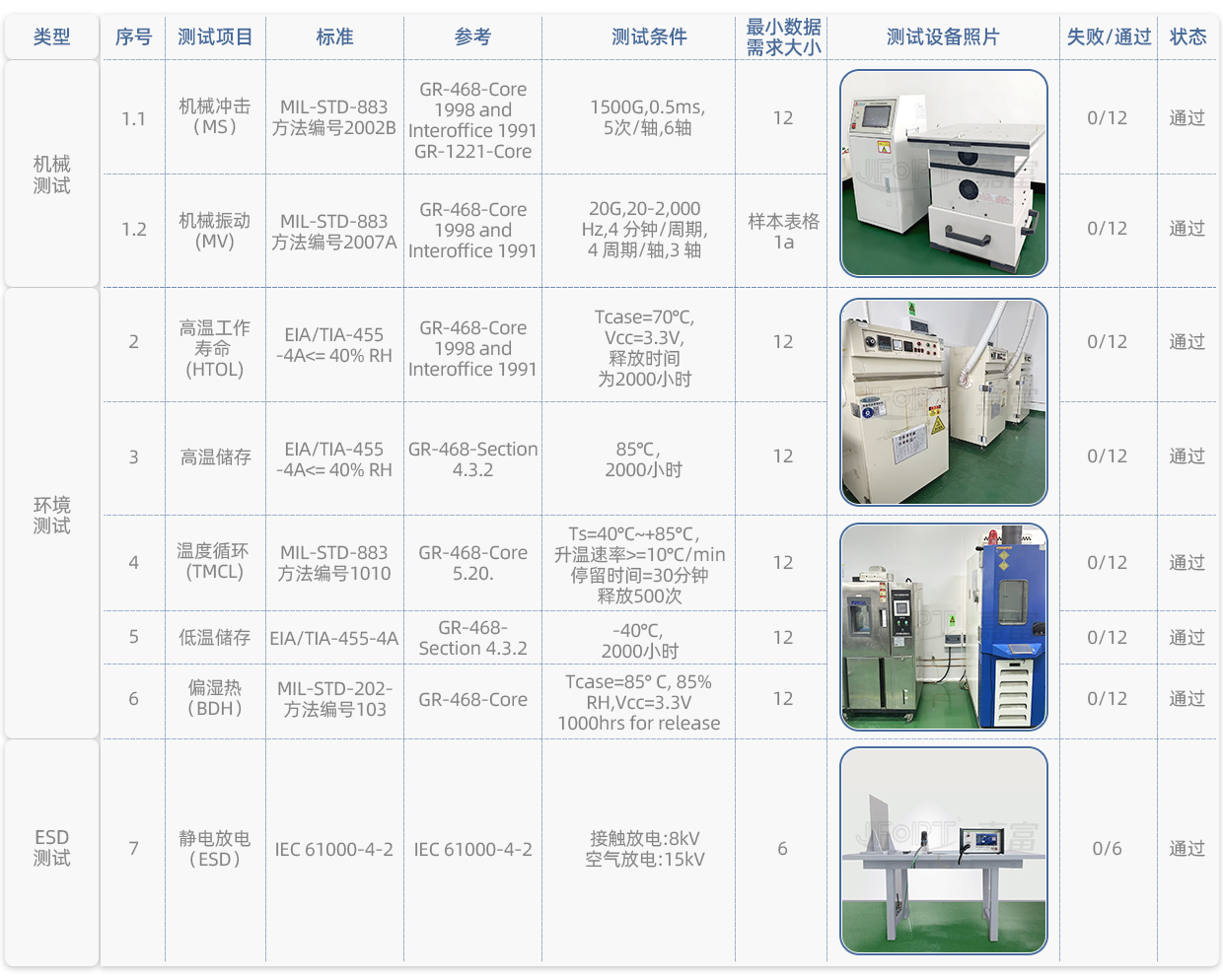
生产及检测设备
PRODUCTION & TESTING EQUIPMENT
产品特点
FEATURES
| Hot Pluggable QSFP+ form factor | Maximum link length of 2km on Single Mode Fiber (SMF) | ||||||||
| Commercial operating case temperature range: 0°C to 70°C | Supports 41.2 Gb/s aggregate bit rates | ||||||||
| Uncooled 4x10Gb/s CWDM transmitter | RoHS-6 Compliant | ||||||||
| Power dissipation <3.5W | XLPPI electrical interface | ||||||||
| Built-in digital diagnostic functions,including optical power monitoring | Single 3.3V power supply | ||||||||
| Duplex LC receptacles |
应用范围
APPLICATION

符合标准
STANDARD COMPLIANCE

绝对最大额定值
ABSOLUTE MAXIMUM RATINGS
| Parameter | Symbol | Min | Typ. | Max | Unit | Ref. | ||
| Maximum supply voltage | Vcc1, VccTx, VccRx | -0.5 | - | 3.6 | V | - | ||
| Supply voltage | Ts | -40 | - | +85 | °C | - | ||
| Case operating temperature | Top | +15 | - | +60 | °C | - | ||
| Relative humidity | RH | 0 | - | 85 | % | 1 | ||
| Damage threshold, per lane | DT | 3.4 | - | - | dBm | - | ||
Note:
1.Non-condensing.
建议操作条件
ELECTRICAL CHARACTERISTICS
| Parameter | Symbol | Min | Typ. | Max | Unit | Ref. | ||
| Supply voltage | Vcc1, VccTx, VccRx | 3.1 | - | 3.47 | V | - | ||
| Supply current | Icc | - | - | 1.13 | A | - | ||
| Transmit turn-on time | - | - | - | 2000 | ms | 1 | ||
Transmitter (per lane) |
||||||||
| Single ended input voltage tolerance | VinT | -0.3 | - | 4.0 | V | - | ||
| Differential data input swing | Vin,pp | 120 | - | 1200 | mVpp | 2 | ||
| Differential input threshold | - | - | 50 | - | mV | - | ||
| AC common mode input voltage tolerance (RMS) |
- | 15 | - | - | mV | - | ||
| J2 jitter tolerancez | Jt2 | 0.17 | - | - | UI | - | ||
| J9 jitter tolerance | Jt9 | 0.29 | - | - | UI | - | ||
| Data dependent pulse width shrinkage | DDPWS | 0.07 | - | - | UI | - | ||
| Eye mask colordinates {X1, X2 ,Y1, Y2} |
- | - | 0.11, 0.31 95, 350 |
- | UI mV |
4 | ||
Receiver (per lane) |
||||||||
| Single-ended output voltage | - | -0.3 | - | 4.0 | V | - | ||
| Differential data output swing | Vout,pp | 200 | - | 400 | mVpp | 5,6 | ||
| 300 | - | 600 | ||||||
| 400 | 550 | 800 | ||||||
| 600 | 1200 | |||||||
| AC common mode output voltage (RMS) |
- | - | - | 7.5 | mV | - | ||
| Termination mismatch at 1 MHx | - | - | - | 5 | % | - | ||
| Differential output return loss | - | Per IEEE P802.3ba,Section 86A.4.2.1 | dB | 3 | ||||
| Common mode output return loss | - | Per IEEE P802.3ba,Section 86A.4.2.2 | dB | 3 | ||||
| Output transition time, 20% to 80% | - | 28 | - | - | ps | - | ||
| J2 jitter output | Jo2 | - | - | 0.42 | UI | - | ||
| J9 jitter output | Jo9 | - | - | 0.65 | UI | - | ||
| Eye mask coordinates #1 {X1, X2, Y1, Y2} |
- | - | 0.29, 0.5 150, 425 |
- | UI mV |
4 | ||
| Power supply ripple tolerance | PSR | 50 | - | - | mVpp | - | ||
Notes:
1.From power-on and end of any fault conditions.
2.After internal AC coupling. Self-biasing 100Ωdifferential input.
3.10 MHz to 11.1 GHz range
4.Hit ratio = 5 x 10E-5.
5.AC coupled with 100Ωdifferential output impedance.
6.Output voltage is settable in 4 discrete steps via the I2C. Default is 400-800 mV.
光电特性
OPTICAL CHARACTERISTICS
| Parameter | Symbol | Min | Typ. | Max | Unit | Ref. | ||
Transmitter (per lane) |
||||||||
| Signaling speed per lane | - | - | - | 10.3125 | GBd | 1 | ||
| Lane center wavelengths (range) | - | 1264.5-1277.5 1284.5-1297.5 1304.5-1317.5 1324.5-1337.5 |
nm | - | ||||
| Total average launch power | Pout | - | - | 8.3 | dBm | - | ||
| Average launch power per lane | TXPx | -7.0 | - | 2.3 | dBm | - | ||
| Transmit OMA per lane | TxOMA | -4.0 | - | 3.5 | dBm | 2 | ||
| Optical extinction ratio | ER | 3.5 | - | - | dB | - | ||
| Sidemode suppression ratio | SSRmin | 30 | - | - | dB | - | ||
| Average launch power of OFF transmitter, per lane | - | - | - | -30 | dBm | - | ||
| Relative intensity tolerance | RIN | - | - | -128 | dB/Hz | 3 | ||
| Optical return loss tolerance | - | - | - | 20 | - | - | ||
| Transmitter reflectance | - | - | - | -12 | dB | - | ||
| Transmitter eye mask definition {X1, X2, X3, Y1, Y2, Y3} |
- | (0.25, 0.4, 0.45, 0.25, 0.28, 0.4) |
- | - | - | - | ||
| - | - | - | - | - | - | - | ||
| Parameter | Symbol | Min | Typ. | Max | Unit | Ref. | ||
Receiver (per lane) |
||||||||
| Signaling speed per lane | - | - | - | 10.3125 | GBd | 4 | ||
| Lane center wavelengths (range) | - | 1264.5-1277.5 1284.5-1297.5 1304.5-1317.5 1324.5-1337.5 |
nm | - | ||||
| Receive power (OMA) per lane | RxOMA | - | - | 3.5 | dBm | - | ||
| Average receive power per lane | RXPx | -11.5 | - | 2.3 | dBm | 5 | ||
| Receiver sensitivity (OMA) per lane |
Rxsens | - | - | -11.5 | dBm | - | ||
| Stressed receiver sensitivity (OMA) per lane |
SRS | - | - | -9.6 | dBm | - | ||
| Damage threshold per lane | PMAX | - | - | 3.4 | dBm | - | ||
| Return loss | RL | - | - | -26 | dB | - | ||
| Vertical eye closure penalty, per lane | - | - | - | 1.9 | dB | - | ||
| Receive electrical 3dB upper cutoff frequency, per lane | - | - | - | 12.3 | GHz | - | ||
| LOS De-assert | LOSD | - | - | -15 | dBm | - | ||
| LOS assert | LOSA | -28 | - | - | dBm | - | ||
| LOS hysteresis | - | - | 1 | - | dB | - | ||
Notes:
1.Transmitter consists of 4 lasers operating at 10.3Gb/s each.
2.Minimum value is informative.
3.RIN is scaled by 10*log(10/4) to maintain SNR outside of transmitter.
4.Receiver consists of 4 photodetectors operating at 10.3Gb/s each.
5.Minimum value is informative, equals min TxOMA with infinite ER and max channel insertion loss.
引脚说明
PIN DESCRIPTION
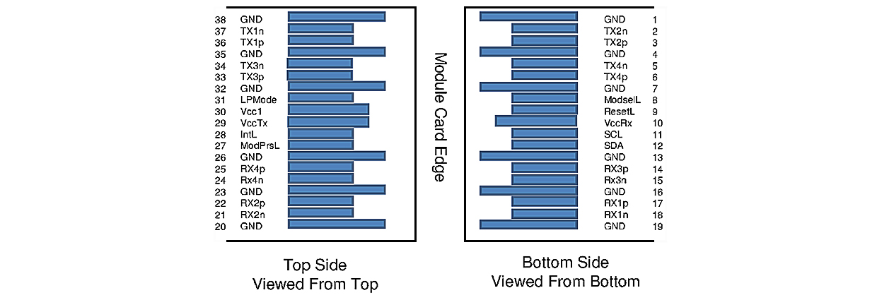
QSFP+ MSA-compliant 38-pin connector
| Pin | Symbol | Name/Description | Notes | |||||
| 1 | GND | Ground | 1 | |||||
| 2 | Tx2n | Transmitter Inverted Data Input | ||||||
| 3 | Tx2p | Transmitter Non-Inverted Data Input | ||||||
| 4 | GND | Ground | 1 | |||||
| 5 | Tx4n | Transmitter Inverted Data Input | ||||||
| 6 | Tx4p | Transmitter Non-Inverted Data Input | ||||||
| 7 | GND | Ground | 1 | |||||
| 8 | ModSelL | Module Select | ||||||
| 9 | ResetL | Module Reset | ||||||
| 10 | Vcc Rx | +3.3V Power Supply Receiver | ||||||
| 11 | SCL | 2-wire Serial Interface Clock | ||||||
| 12 | SDA | 2-wire Serial Interface Data | ||||||
| 13 | GND | Ground | 1 | |||||
| 14 | Rx3p | Receiver Non-Inverted Data Output | ||||||
| 15 | Rx3n | Receiver Inverted Data Output | ||||||
| 16 | GND | Ground | 1 | |||||
| 17 | Rx1p | Receiver Non-Inverted Data Output | ||||||
| 18 | Rx1n | Receiver Inverted Data Output | ||||||
| 19 | GND | Ground | 1 | |||||
| 20 | GND | Ground | 1 | |||||
| 21 | Rx2n | Receiver Inverted Data Output | ||||||
| 22 | Rx2p | Receiver Non-Inverted Data Output | ||||||
| 23 | GND | Ground | 1 | |||||
| 24 | Rx4n | Receiver Inverted Data Output | ||||||
| 25 | Rx4p | Receiver Non-Inverted Data Output | ||||||
| 26 | GND | Ground | 1 | |||||
| 27 | ModPrsL | Module Present | ||||||
| 28 | IntL | Interrupt | ||||||
| 29 | Vcc Tx | +3.3V Power Supply Transmitter | ||||||
| 30 | Vcc1 | +3.3V Power Supply | ||||||
| 31 | LPMode | Low Power Mode | ||||||
| 32 | GND | Ground | ||||||
| 33 | Tx3p | Transmitter Non-Inverted Data Input | 33 | |||||
| 34 | Tx3n | Transmitter Inverted Data Input | ||||||
| 35 | GND | Ground | 1 | |||||
| 36 | Tx1p | Transmitter Non-Inverted Data Input | ||||||
| 37 | Tx1n | Transmitter Inverted Data Input | ||||||
| 38 | GND | Ground | 1 | |||||
Note:
Circuit ground is internally isolated from chassis ground.
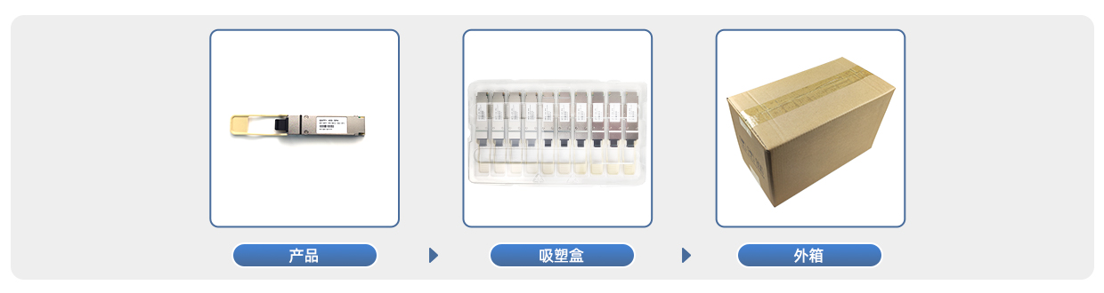
产品包装
PRODUCT PACKAGING
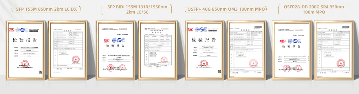
产品认证
PRODUCT CERTIFICATION
质量优势
QUALITY ADVANTAGE
兼容品牌
COMPATIBLE BRANDS


 Wendy
Wendy Sophie
 Jeanne


