


|
产品型号
|
JFTSM-QSFP+40-85-015(SR)-MPO8/12
|
工厂品牌
|
JFOPT嘉富
|
|
封装形式
|
QSFP+
|
光口类型
|
MPO 8C/12C
|
|
最高总速率
|
40G
|
每通道速率
|
10.3125Gbps
|
|
OM3最大传输距离
|
100m
|
OM4最大传输距离
|
150m
|
|
工作波长
|
850nm
|
工作电压
|
3.3V
|
|
光纤型号
|
MMF
|
纤芯尺寸
|
50/125
|
|
发射器类型
|
VCSEL
|
接收器类型
|
PIN
|
|
发射功率
|
-7.6~2.4dbm
|
接收灵敏度
|
-5.4dbm
|
|
数字诊断(DDM)
|
YES
|
接收过载
|
2.4dBm
|
|
功耗
|
< 1.5W
|
支持协议
|
IEEE 802.3ba
IEEE 802.3ae
QSFP+ MSA SFF-8436
|
|
工作温度(商业级)
|
0℃~+70℃
|
储存温度(商业级)
|
-40℃~+85℃
|
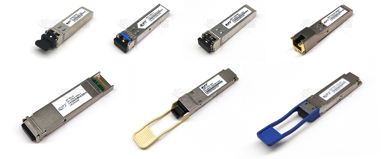
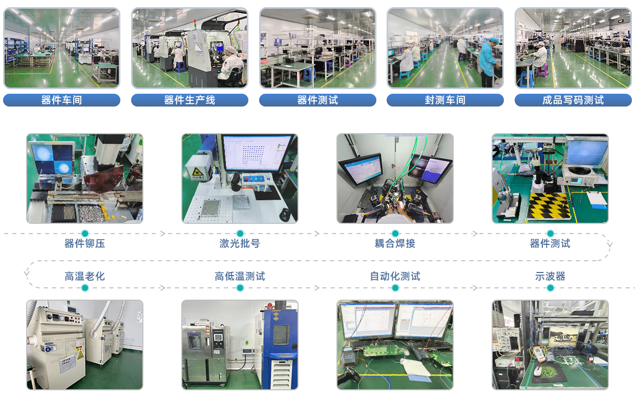
JFOPT嘉富持续投入光模块生产领域,产品覆盖1*9、SFP、10G、25G、100G、200G、400G、800G GPON/EPON/XG/XGSPON OLT等全系列光模块。同时为下游同行提供TOSA、ROSA、BOSA等光器件半成品解决方案。JFOPT嘉富生产线具备日产量一万只光模块、两万只光器件的能力。此外,JFOPT嘉富光模块拥有业界领先的耐高温、抗干扰特性,广泛应用于计算中心、运营商、交通安防、电力设施等行业领域。
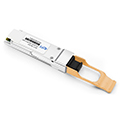
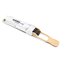
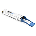
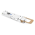
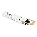
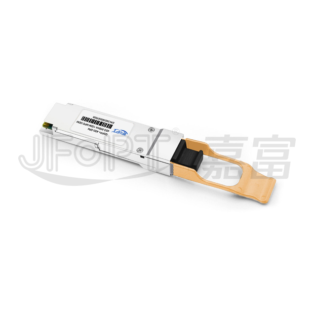
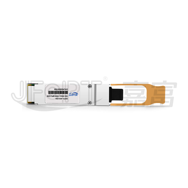
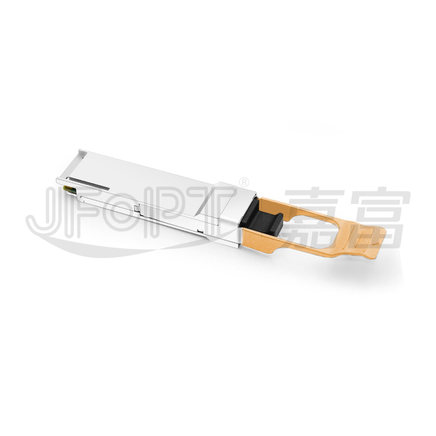
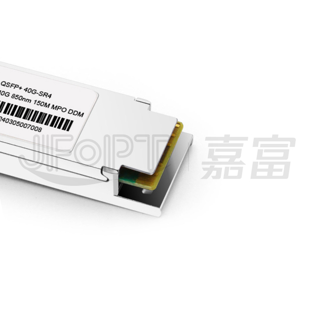
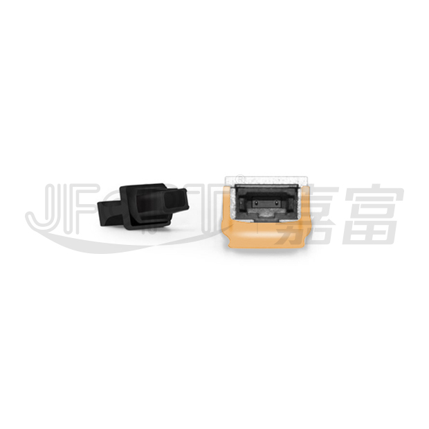
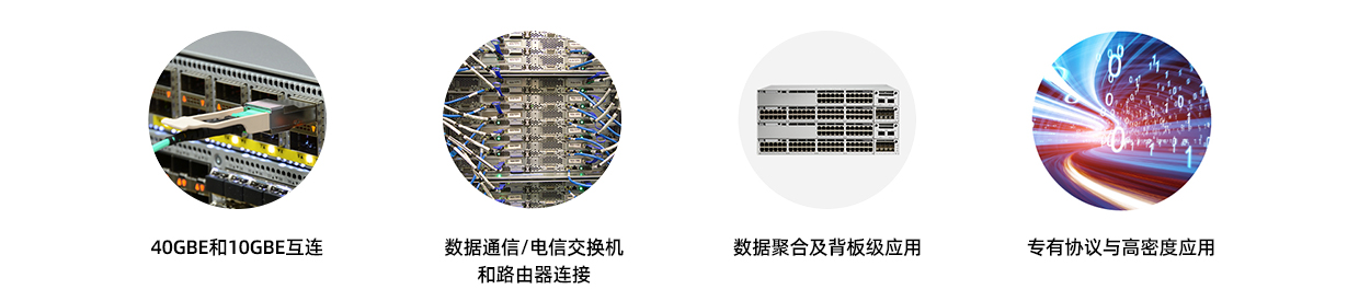
JFOPT QSFP+ 40G 850nm 150米 SR MPO8/12光模块配备12芯MTP/MPO公头连接器,支持通过OM4多模光纤传输150米,通过OM3多模光纤传输100米。该模块符合QSFP+ MSA标准和IEEE 802.3ba 40GBASE-SR4规范,并支持4x10GBASE-SR分路传输。在完全兼容标准40GBASE-SR4接口的同时,还基于QSFP+ MSA规范通过I2C接口提供数字诊断功能,可实时获取运行参数。其热插拔和易安装特性使其成为园区网、数据中心、云部署、高性能计算(HPC)环境以及交换机/路由器/服务器/传输设备间互连等广泛应用的理想选择。
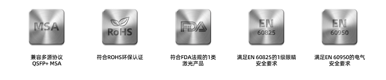
| Compliant to the IEEE 802.3ba(40GBASE-SR4) | Support interoperability with IEEE 802.3ae,10GBASE-SR modules of various form factors such as SFP+, XFP, X21 | ||||||||
| Compliant to the QSFP+ MSA SFF-8436 Specification | Up to 100m on OM3 and 150m on OM4 MMF | ||||||||
| VCSEL array transmitter and PIN array receiver | Single 3.3V Power Supply and Power dissipation < 1.5W | ||||||||
| Operates at 10.3125Gbps per channel | Operating Case Temperature: 0℃~+70℃ | ||||||||
| I2C interface with integrated Digital Diagnostic Monitoring | Utilizes a standard 12/8 lane optical fiber with MPO connector | ||||||||
| Safety Certification: TUV/UL/FDA |
| Parameter | Symbol | Min. | Max. | Unit | ||||
| Storage Temperature | TS | -40 | +85 | °C | ||||
| Supply Voltage | VCC | -0.5 | 3.6 | V | ||||
| Operating Relative Humidity | RH | 5 | 85 | % | ||||
| *Exceeding any one of these values may destroy the device immediately. |
||||||||
| Parameter | Symbol | Min. | Typical | Max. | Unit | |||
| Operating Case Temperature | Tc | JFTSM-QSFP+40-85-015(SR)-MPO8/12 | 0 | +70 | °C | |||
| Power Supply Voltage | Vcc | 3.135 | 3.3 | 3.465 | V | |||
| Power Supply Current | Icc | 450 | mA | |||||
| Aggregate Bit Rate | BRAVE | 41.25 | Gbps | |||||
| Lane Bit Rate | BRLANE | 10.3125 | Gbps | |||||
| Parameter |
Symbol
|
Min. | Typical | Max. | Unit | |||
| OM3 MMF | L | 0.5 | - | 100 | m | |||
| Aggregate Bit Rate | BRAVE | - | 40 | - | Gbps | |||
| Per Lane Bit Rate | BRLANE | - | 10.3125 | - | Gbps | |||
Transmitter |
||||||||
| Center Wavelength | λC | 840 | 850 | 860 | nm | |||
| RMS Spectral Width | RMS | - | - | 0.65 | nm | |||
| Average Launch Power, Each Lane | Pout/lane | -7.6 | - | 2.4 | dBm | |||
| Transmit OMA, Per Lane | TX_OMA/lane | -5.6 | - | 3 | dBm | |||
| Difference in Launch Power Between Any Two Lanes(OMA) | - | - | 4 | dB | ||||
| Peak Power, Each Lane | - | - | 4 | dBm | ||||
| Transmitter and Dispersion Penalty,Each Lane | TDP/lane | - | - | 3.5 | dB | |||
| Extinction Ratio | ER | 3 | - | - | dB | |||
| Optical Return Loss Tolerance | - | - | 12 | dB | ||||
| Average Launch Power of OFF, Each Lane | - | - | -30 | dBm | ||||
| Output Optical Eye | IEEE 802.3ba-2010 Compliant | |||||||
Receiver |
||||||||
| Center Wavelength | λC | 840 | 850 | 860 | nm | |||
| Damage Threshold | 3.4 | - | - | dB | ||||
| Stressed Receiver Sensitivity in OMA,Each Lane | Pmins | - | - | -5.4 | dBm | |||
| Maximum Receive Power, Each Lane | Pmax | - | - | 2.4 | dBm | |||
| Average Power, Each Lane | RX/lane | -9.5 | - | +2.4 | dBm | |||
| LOS De-Assert, OMA | LOSD | - | - | -7.5 | dBm | |||
| Receiver Reflectance | Rr | - | - | -12 | dB | |||
| LOS Assert | LOSA | -30 | - | - | dBm | |||
| LOS Hysteresis | 0.5 | - | - | dB | ||||
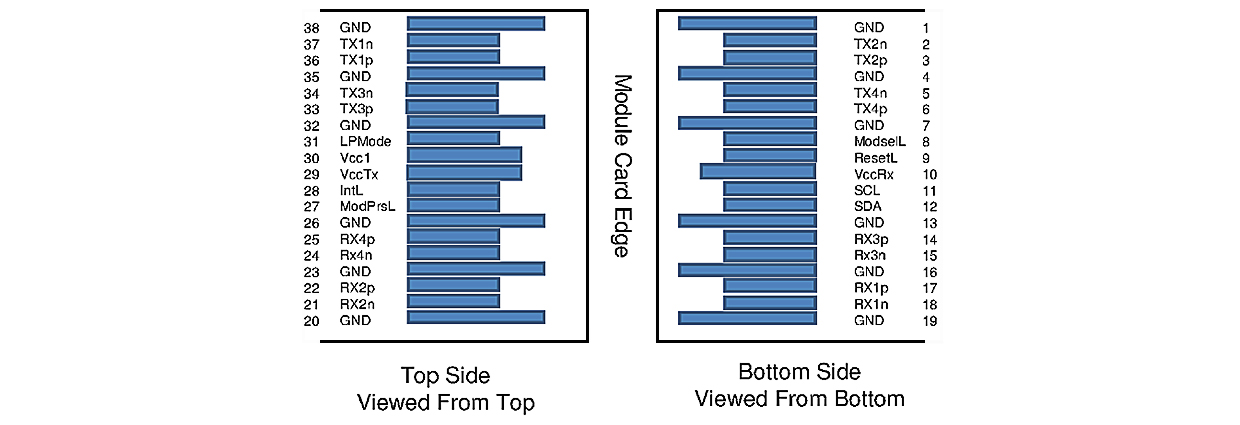
| Pin | Logic | Symbol | Description | Plug Sequence |
Notes | |||
| 1 | GND | Ground | 1 | 1 | ||||
| 2 | CML-I | Tx2n | Transmitter Inverted Data Input | 3 | ||||
| 3 | CML-I | Tx2p | Transmitter Non-Inverted Data Input | 3 | ||||
| 4 | GND | Ground | 1 | 1 | ||||
| 5 | CML-I | Tx4n | Transmitter Inverted Data Input | 3 | ||||
| 6 | CML-I | Tx4p | Transmitter Non-Inverted Data Input | 3 | ||||
| 7 | GND | Ground | 1 | 1 | ||||
| 8 | LVTTL-I | ModSelL | Module Select | 3 | ||||
| 9 | LVTTL-I | ResetL | Module Reset | 3 | ||||
| 10 | VccRx | +3.3V Power Supply Receiver | 2 | 2 | ||||
| 11 | LVCMOS- I/O | SCL | 2-wire Serial Interface Clock | 3 | ||||
| 12 | LVCMOS- I/O | SDA | 2-wire Serial Interface Data | 3 | ||||
| 13 | GND | Ground | 1 | 1 | ||||
| 14 | CML-O | Rx3p | Receiver Non-Inverted Data Output | 3 | ||||
| 15 | CML-O | Rx3n | Receiver Inverted Data Output | 3 | ||||
| 16 | GND | Ground | 1 | 1 | ||||
| 17 | CML-O | Rx1p | Receiver Non-Inverted Data Output | 3 | ||||
| 18 | CML-O | Rx1n | Receiver Inverted Data Output | 3 | ||||
| 19 | GND | Ground | 1 | 1 | ||||
| 20 | GND | Ground | 1 | 1 | ||||
| 21 | CML-O | Rx2n | Receiver Inverted Data Output | 3 | ||||
| 22 | CML-O | Rx2p | Receiver Non-Inverted Data Output | 3 | ||||
| 23 | GND | Ground | 1 | 1 | ||||
| 24 | CML-O | Rx4n | Receiver Inverted Data Output | 3 | ||||
| 25 | CML-O | Rx4p | Receiver Non-Inverted Data Output | 3 | ||||
| 26 | GND | Ground | 1 | 1 | ||||
| 27 | LVTTL-O | ModPrsL | Module Present | 3 | ||||
| 28 | LVTTL-O | IntL | Interrupt | 3 | ||||
| 29 | VccTx | +3.3V Power supply transmitter | 2 | 2 | ||||
| 30 | Vcc1 | +3.3V Power supply | 2 | 2 | ||||
| 31 | LVTTL-I | LPMode | Low Power Mode | 3 | ||||
| 32 | GND | Ground | 1 | 1 | ||||
| 33 | CML-I | Tx3p | Transmitter Non-Inverted Data Input | 3 | ||||
| 34 | CML-I | Tx3n | Transmitter Inverted Data Input | 3 | ||||
| 35 | GND | Ground | 1 | 1 | ||||
| 36 | CML-I | Tx1p | Transmitter Non-Inverted Data Input | 3 | ||||
| 37 | CML-I | Tx1n | Transmitter Inverted Data Input | 3 | ||||
| 38 | GND | Ground | 1 | 1 | ||||
1: GND is the symbol for signal and supply (power) common for the QSFP+ module. All are common within the QSFP+ module and all module voltages are referenced to this potential unless otherwise noted. Connect these directly to the host board signal-common ground plane.
2: Vcc Rx, Vcc1 and Vcc Tx are the receiver and transmitter power supplies and shall be applied concurrently. Vcc Rx Vcc1 and Vcc Tx may be internally connected within the QSFP+ Module in any combination. The connector pins are each rated for a maximum current of 500mA.


 Wendy
Wendy Sophie
 Jeanne


