


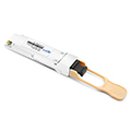
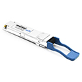
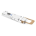
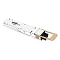
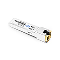


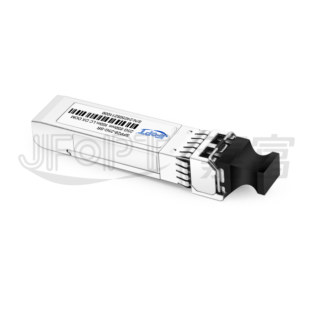
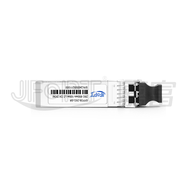
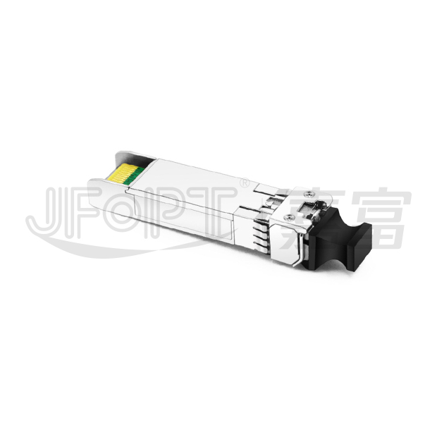
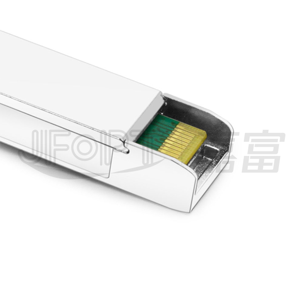

| 产品型号 | JFTSM-SFP28-25-85-01(SR)-LCD | 工厂品牌 | JFOPT嘉富 |
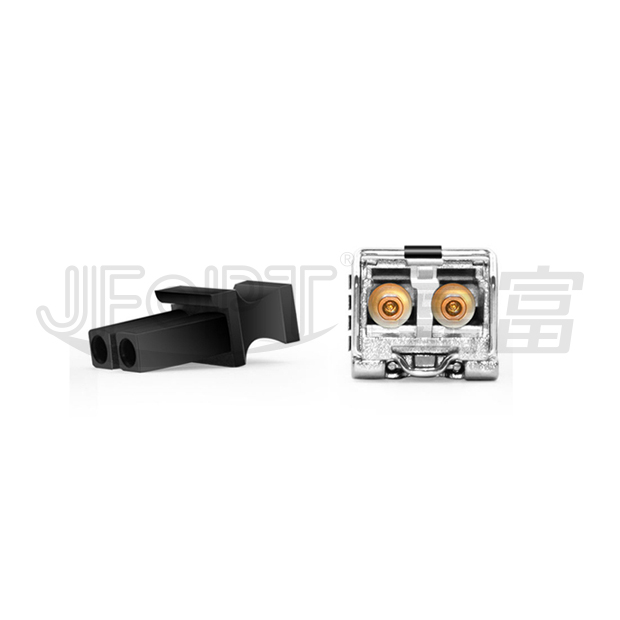
| 封装形式 | SFP28 | 光口类型 | LC 双联 |
| 最高总速率 | 25.78G | 每通道速率 | 10.31Gbps |
| OM3最大传输距离 | 70m | OM4最大传输距离 | 100m |
| 工作波长 | 850nm | 工作电压 | 3.3V |
| 光纤型号 | MMF | 纤芯尺寸 | 50/125 |
| 发射器类型 | VCSEL | 接收器类型 | PIN |
| 发射功率 | -8.4~2.4dbm | 接收灵敏度 | <-6dBm |
| 数字诊断(DOM) | YES | 接收过载 | 2.4dBm |
| 功耗 | ≤1W | 支持协议 | SFF-8472, SFF-8024, SFF-8431, SFF-8432 |
| 工作温度(商业级) | 0℃~+70℃ | 储存温度(商业级) | -40℃~+85℃ |
| 工作温度(工业级) | -40℃~+85℃ | 储存温度(工业级) | -40℃~+85℃ |
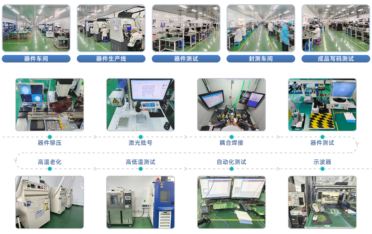
生产线介绍
PRODUCTION LINE INTRODUCTION
JFOPT嘉富持续投入光模块生产领域,产品覆盖1*9、SFP、10G、25G、100G、200G、400G、800G GPON/EPON/XG/XGSPON OLT等全系列光模块。同时为下游同行提供TOSA、ROSA、BOSA等光器件半成品解决方案。JFOPT嘉富生产线具备日产量一万只光模块、两万只光器件的能力。此外,JFOPT嘉富光模块拥有业界领先的耐高温、抗干扰特性,广泛应用于计算中心、运营商、交通安防、电力设施等行业领域。
产品介绍
PRODUCT PRESENTATION
JFOPT SFP28 25G 850nm 100m SR LC DX光模块专为多模光纤上的25.78Gbps数据传输而优化设计,完全符合SFF-8431标准,其SFP+机械结构兼容SFF-8432规范。该模块支持通过双线串行接口实现数字诊断监控功能(遵循SFF-8472标准),从而确保精准的性能监测并简化网络管理。
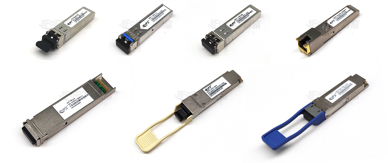
光模块系列产品
TRANSCEIVER SERIES PRODUCTS
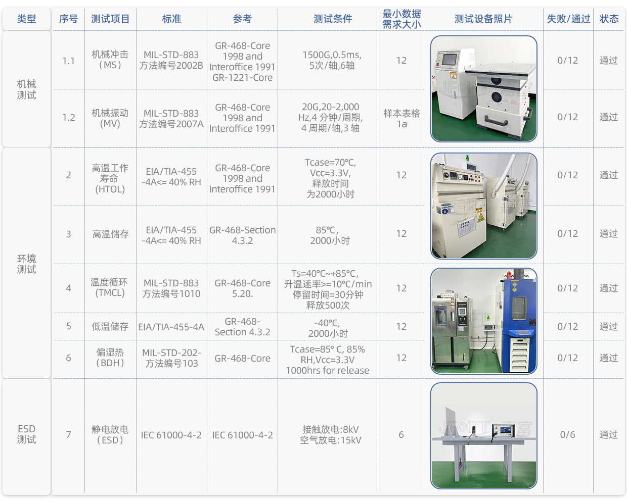
生产及检测设备
PRODUCTION & TESTING EQUIPMENT
产品特点
FEATURES
| Supports 25.78Gb/s bit rate | Hot-pluggable SFP+ footprint | ||||||||
| 850nm VCSEL laser and PIN photo-detector | Internal CDR on transmitter and receiver channel | ||||||||
| Programmable RX pre-emphasis | Programmable TX input equalizer | ||||||||
| 0℃ to 70℃ operating temperature range | Link lengths at 25.78G 100m over OM4 MMF | ||||||||
| Single +3.3V±5% power supply |
应用范围
APPLICATION
| 25GBASE-SR ethernet |
符合标准
STANDARD COMPLIANCE

绝对最大额定值
ABSOLUTE MAXIMUM RATINGS
| Parameter | Symbol | Min. | Max. | Unit | |||||
| Supply voltage | Vcc | -0.3 | +4.0 | V | |||||
| Storage temperature | Ts | -40 | +85 | ℃ | |||||
| Operating humidity | RH | 0 | +85 | % | |||||
一般规范
GENERAL SPECIFICATIONS
| Parameter | Symbol | Min | Typ. | Max | Unit | ||||
| Bit rate | BR | - | 25.78 | - | Gbps | ||||
| Bit Error ratio | BER | - | - | 5*10E-5 | - | ||||
| Max. supported link length | LMax | - | - | 100 | m | ||||
建议操作条件
RECOMMENDED OPERATING CONDITIONS
| Parameter | Symbol | Min. | Typ. | Max. | Unit | ||||
| Operating temperature | Tc | 0 | - | +70 | °C | ||||
| Power supply voltage | Vcc | 3.1 | 3.3 | 3.46 | V | ||||
| Bit rate | BR | - | 25.78 | - | Gbps | ||||
| Max. supported link length | LMAX | - | - | 100 | m | ||||
电气特性
ELECTRICAL CHARACTERISTICS
| Parameter | Symbol | Min. | Typ. | Max | Unit | Note | |||
| Supply voltage | Vcc | 3.14 | 3.3 | 3.46 | V | - | |||
| Supply current | Icc | - | - | 230 | mA | - | |||
Transmitter |
|||||||||
| Input differential impedance | RIN | 80 | 100 | 120 | Ω | 1 | |||
| Single ended data input swing | VIN | 90 | - | 150 | mVp-p | - | |||
| Transmit disable voltage | VDIS | 2 | - | VCCHOST | V | - | |||
| Transmit enable voltage | VEN | VEE | - | VEE+0.8 | V | - | |||
| Transmit fault assert voltage | VFA | 2 | - | VCCHOST | V | - | |||
| Transmit fault de-assert voltage | VFDA | VEE | - | VEE+0.8 | V | - | |||
Receiver |
|||||||||
| Single ended data output swing | VOD | 200 | - | 500 | mVpp | - | |||
| LOS fault | VLOSFT | 2 | - | VCCHOST | V | - | |||
| LOS normal | VLOSFT | VEE | - | VEE+0.8 | V | - | |||
光学特性
OPTICAL CHARACTERISTICS
| Parameter | Symbol | Min. | Typ. | Max. | Unit | Note | |||
Transmitter |
|||||||||
| Nominal wavelength | λ | 840 | - | 860 | nm | - | |||
| Spectral width | ∆λ | - | - | 0.6 | nm | - | |||
| Optical modulation amplitude | POMA | -6.4 | - | 3 | dBm | - | |||
| Optical output power | POFF | -8.4 | - | 2.4 | dBm | - | |||
| Extinction ratio | ER | 2 | - | - | dB | - | |||
| Transmitter dispersion penalty | TDP | - | - | 5 | dB | - | |||
| Average launch power of OFF Transmitter |
POFF | - | - | -30 | dBm | - | |||
Receiver |
|||||||||
| Center wavelength | λ | 840 | - | 860 | nm | - | |||
| Average receiver power | PAVG | -10.3 | - | 2.4 | dBm | 1 | |||
| Stressed receiver sensitivity(OMA) | RSENSE | - | - | -5.2 | dBm | 2 | |||
| Receiver reflectance | RREFL | - | - | -12 | dB | - | |||
| Assert LOS | LOSA | -30 | - | - | dBm | - | |||
| De-assert LOS | LOSD | - | - | -13 | dBm | - | |||
| LOS hysteresis | 0.5 | dB | - | ||||||
| Notes: 1. Sensitivity for 25.78G PRBS 231-1 and BER better than or equal to 5*10E-5. 2. The stressed sensitivity values in the table are for system level BER measurements which include the effects of CDR circuit. |
|||||||||
引脚分配
PIN ASSIGNMENT

| Pin Number | Symbol | Name | Description | ||||||
| 1,17,20 | VeeT | Transmitter signal ground | These pins should be connected to signal groundon the host board. | ||||||
| 2 | TX fault | Transmitter fault out (OC) | Logic “1” output = Transmitter fault Logic “0” output = Normal operation This pin is open collector compatible, and should be pulled up to host Vcc with a 10kΩ resistor. |
||||||
| 3 | TX disable | Transmitter disable in (LVTTL) | Logic “1” input (or no connection) = Laser off Logic “0” Input = Laser on This pin is internally pulled up to VccT with a 10 kΩ resistor |
||||||
| 4 | SDA | Module definition identifiers | Serial ID with SFF 8472 diagnostics module definition pins should be pulled up to Host Vcc with 10 kΩ resistors. | ||||||
| 5 | SCL | ||||||||
| 6 | MOD-ABS | ||||||||
| 7 | RS0 | Receiver rate select (LVTTL) Transmitter rate select (LVTTL) |
NA | ||||||
| 9 | RS1 | NA | |||||||
| 8 | LOS | Loss of signal out (OC) | This pin is open collector compatible, and should be pulled up to host Vcc with a 10kΩ resist |
||||||
| 10,11,14 | VeeR | Receiver signal ground | These pins should be connected to signal groundon the host board. | ||||||
| 12 | RD- | Receiver negative DATA out (CML) | Light on = logic “0” output receiver DATA output is internally AC coupled and series terminated with a 50Ω resistor. | ||||||
| 13 | RD+ | Receiver positive DATA out(CML) | Light on = Logic “1” output receiver DATA output is internal ly AC coupled and series terminated with a 50 Ω resistor. |
||||||
| 15 | VccR | Receiver power supply | This pin should be connected to a filtered +3.3V power supply on the host board. See figure 3.recommended power supply filter | ||||||
| 16 | VccT | Transmitter power supply | This pin should be connected to a filtered +3.3V power supply on the host board. See figure 3.recommended power supply filter | ||||||
| 18 | TD+ |
Transmitter positive DATA in(CML)
|
Logic “1” input = light on transmitter DATA inputs are internally AC coupled and terminated with a differential 100Ω resistor. | ||||||
| 19 | TD- | Transmitter negative DATA in(CML) | Logic “0” input = light on transmitter DATA inputs are internally AC coupled and terminated with a differential 100Ω resistor. | ||||||
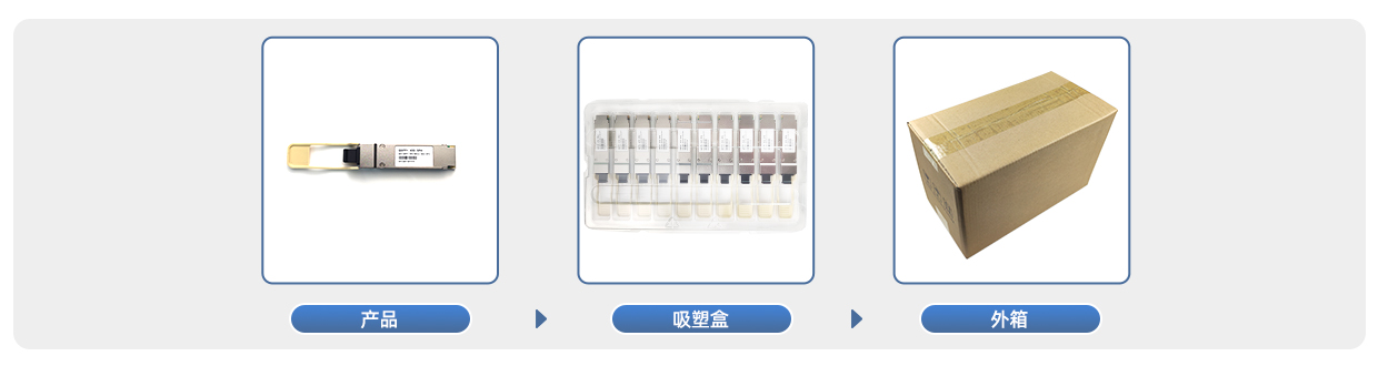
产品包装
PRODUCT PACKAGING
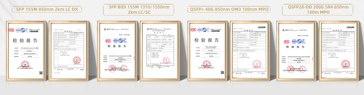
产品认证
PRODUCT CERTIFICATION
质量优势
QUALITY ADVANTAGE
兼容品牌
COMPATIBLE BRANDS


 Wendy
Wendy Sophie
 Jeanne


