


|
产品型号
|
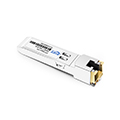
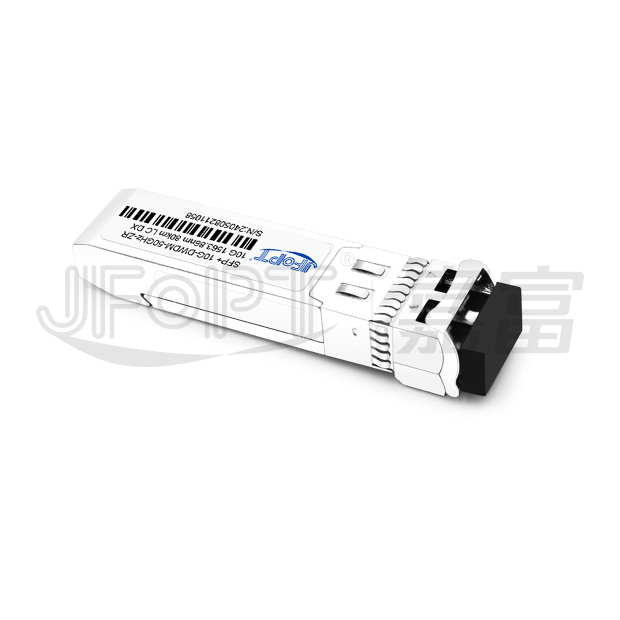
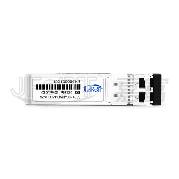
JFTSM-SFP+10-50DW-80(ZR)-LCD
|
工厂品牌
|
JFOPT嘉富
|
|
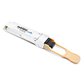
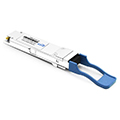
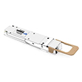
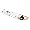
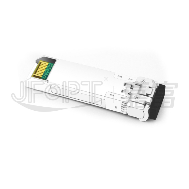
封装形式
|
SFP+
|
光口类型
|
LC Duplex
|
|
最高总速率
|
11.3Gbps
|
每通道速率
|
10.3125Gbps
|
|
最大传输距离
|
80km
|
||
|
工作波长
|
1529.16~1567.13nm((Tunable);1563.86nm-1528.77nm
|
工作电压
|
3.3V
|
|
光纤型号
|
SMF
|
纤芯尺寸
|
9/125
|
|
发射器类型
|
Monolithic MZM Tunable TOSA
|
接收器类型
|
APD
|
|
发射功率
|
-1~3dBm,-1~4dBm;0~5dBm
|
接收灵敏度
|
-23dBm
|
|
数字诊断
|
YES
|
接收过载
|
-7dBm
|
|
功耗
|
C<2.0W,I<2.5W;C<1.65W
|
支持协议
|
SFF-8431
SFF-8472
SFF-8690
ITU-T G.698.1
|
|
工作温度(商业级)
|
0℃~+70℃
|
储存温度(商业级)
|
-40℃~+85℃
|
|
工作温度(工业级)
|
-40℃~+85℃
|
储存温度(工业级)
|
-40℃~+85℃
|
生产线介绍
PRODUCTION LINE INTRODUCTION
JFOPT嘉富持续投入光模块生产领域,产品覆盖1*9、SFP、10G、25G、100G、200G、400G、800G GPON/EPON/XG/XGSPON OLT等全系列光模块。同时为下游同行提供TOSA、ROSA、BOSA等光器件半成品解决方案。JFOPT嘉富生产线具备日产量一万只光模块、两万只光器件的能力。此外,JFOPT嘉富光模块拥有业界领先的耐高温、抗干扰特性,广泛应用于计算中心、运营商、交通安防、电力设施等行业领域。
产品介绍
PRODUCT PRESENTATION
JFOPT SFP+ 10G 50GHz DWDM 80km ZR LC DX收发器是一款高性能高性价比解决方案,支持9.95Gbps-11.3Gbps(带CDR)与8.5Gbps(旁路CDR)多速率传输,在单模光纤(SMF)上实现80公里传输;采用双组件结构:发射端集成激光驱动器与温度调谐光发射次组件(TTOSA),接收端结合雪崩光电二极管(APD)与跨阻放大器(TIA);通过20针连接器热插拔,高速电气接口基于低电压逻辑,具备100欧姆差分阻抗及交流耦合;TX_DIS通过LVTTL高电平禁用光输出,Tx_Fault指示激光器异常,RX_LOS标识输入光信号丢失;内置串行EEPROM支持双线制SFP管理接口监控配置,存储器划分为低位区(存储基础数字诊断(DD)数据)与高位区(特定数据存储于高位内存表)。
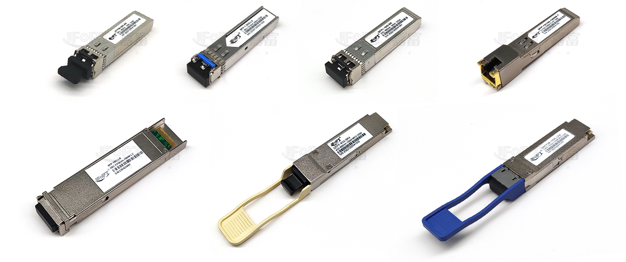
光模块系列产品
TRANSCEIVER SERIES PRODUCTS
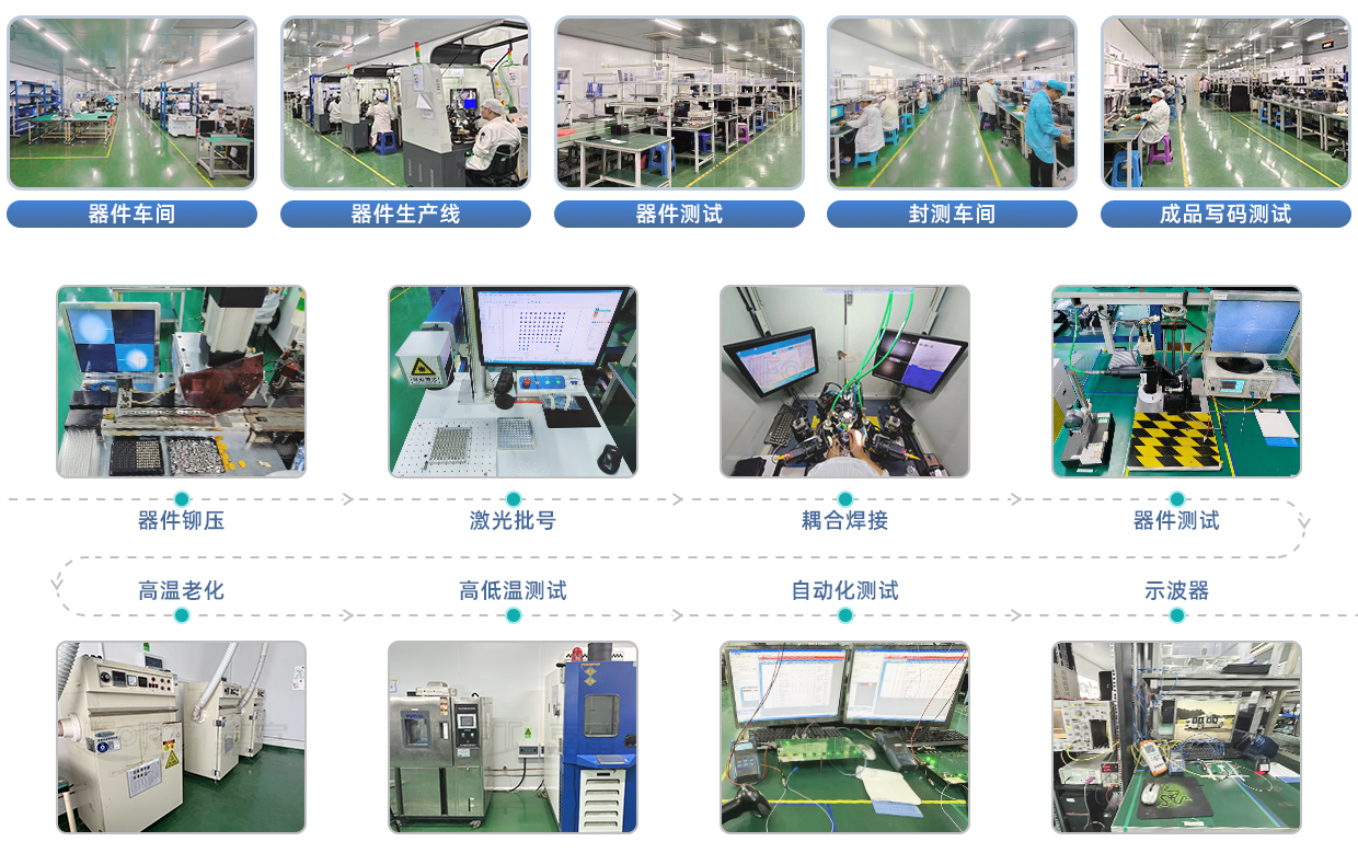
生产及检测设备
PRODUCTION & TESTING EQUIPMENT
产品特点
FEATURES
| Up to 80km transmission on SMF | Support multi rate 9.95Gbps to 11.3Gbps with CDR,8.5Gbps bypass CDR | ||||||||
| Monolithic MZM tunable TOSA | APD receiver | ||||||||
| 50GHz ITU-based channel spacing (C-Band) with a wavelength locker | Total 96 channels | ||||||||
| SFI electrical interface | 2-wire interface for integrated Digital diagnostic monitoring | ||||||||
| SFP+ MSA package with duplex LC conn | Hot pluggable | ||||||||
| Very low EMI and excellent ESD protection | Power consumption less than 2.5W | ||||||||
| Operating case temperature: -5~85°C |
应用范围
APPLICATION
| DWDM 10Gb/s SONET/SDH | DWDM 10Gb/s ethernet & 10Gb/s fibre channel | ||||||||
| DWDM 10Gb/s SONET/SDH w/FEC | DWDM 10Gb/s ethernet & 10Gb/s fibre channel w/FEC |
符合标准
STANDARD COMPLIANCE

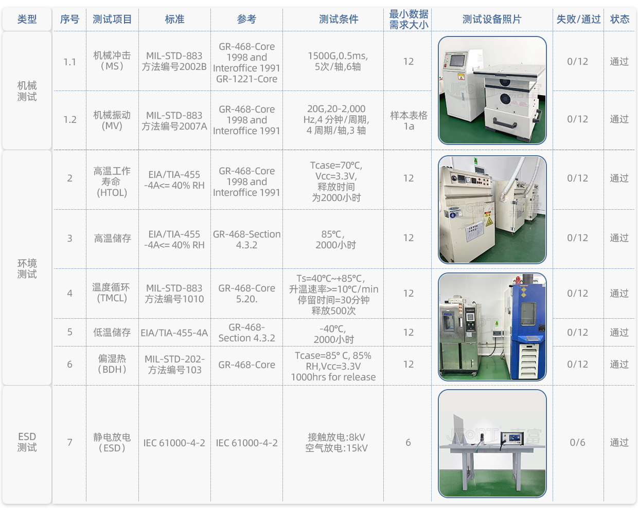
绝对最大额定值
ABSOLUTE MAXIMUM RATINGS
| Parameter | Symbol | Min. | Max. | Unit | Notes | ||||
| Storage temperature | Ts | -40 | 85 | ℃ | - | ||||
| Supply voltage | Vcc3 | 0 | 3.63 | V | - | ||||
| Relative humidity | RH | 5 | +85 | % | Note1 | ||||
建议操作条件
RECOMMENDED OPERSTING CONDITIONS
| Parameter | Symbol | Min. | Typ. | Max. | Unit | Notes | |||
| Operating case temperature | Tc | -5 | 25 | 85 | °C | - | |||
| Supply voltage | Vcc | 3.13 | 3.3 | 3.47 | V | - | |||
| Power consumption | P | - | - | 2.5 | W | - | |||
| Data rate | - | 8.5 | 10.3125 | 11.3 | Gbps | - | |||
| Transmission distance | - | - | - | 80 | Km | - | |||
发射机工作特性 - 光学&电气
TRANSMITTER OPERATING CHARACTERISTIC-OPTICAL & ELECTRICAL
| Parameter | Symbol | Min. | Typical | Max | Unit | Note | |||
| Data rate | DR | 8.5 | 10.3125 | 11.3 | Gbps | - | |||
| Center wavelength | CW | 191.30 | - | 196.05 | THz | - | |||
| Wavelength range | λC | 1529.16 | - | 1567.13 | nm | - | |||
| Center frequqncy variation | CFV | - | - | +/-2.5 | GHz | - | |||
| -20dB spectral width | Δλ20 | - | - | 0.3 | nm | - | |||
| Side mode suppression ratio | SMSR | 30 | - | - | nm | - | |||
| Laser off power | Poff | - | - | -30 | dBm | - | |||
| Optical eye mask | EMM | 5 | - | - | % | - | |||
| Average optical power | PO | -1 | - | 3 | dBm | - | |||
| Extinction ratio | ER | 8.2 | - | dB | - | ||||
| Cross point of eye | CP | 40 | - | 52 | % | - | |||
| Transmitter dispersion renalty | TDP | - | - | 2 | dB | - | |||
| Relative intensity noise | RIN 12OMA | - | - | -128 | dB/Hz | - | |||
| Optical eye mask | ORLT | - | - | -27 | dB | - | |||
| Tx Input diff voltage | VI | 200 | - | 700 | mV | - | |||
接收器工作特性 - 光学&电气
RECEIVER OPERATING CHARACTERISTIC-OPTICAL & ELECTRICAL
| Parameter | Symbol | Min. | Typical | Max. | Unit | Note | |||
| Data rate | DR | 8.5 | 10.3125 | 11.3 | Gbps | - | |||
| Center wavelength | CW | 1260 | - | 1600 | nm | - | |||
| Sensitivity @(BER=1E-12, PRBS 2^31-1, NRZ, 9.95Gbps~10.7Gbps data rate | Psen | - | - | -23 | dBm | - | |||
| Sensitivity @(BER=1.0E-04, PRBS 2^31- 1, NRZ,11.3Gbps data rate) | Psen | - | - | -26 | dBm | - | |||
|
B2B OSNR Tolerance @ 1E-4
|
- | - | - | 16 | dB | - | |||
| Input optical power(no damaged) | IOP | 4 | - | - | dBm | - | |||
| Saturation power(EOL) | SP | -7 | - | - | dBm | - | |||
| Loss of signal - asserted | LosA | -35 | - | - | dBm | - | |||
| Loss of signal - deasserted | LosD | - | - | -28 | dBm | - | |||
| Hysteresis | LosH | 0.5 | - | - | dB | - | |||
| Rx output diff voltage | Vo | 250 | - | 850 | mV | - | |||
| Loss of signal voltage | VOH | Vcc-0.5 | - | Vcc+0.3 | V | - | |||
| VOL | 0 | - | 0.4 | V | - | ||||
数字诊断功能
DIGITAL DIAGNOSTIC FUNCTIONS
| Parameter | Symbol | Min. | Typical | Max | Units | Notes | |||
| Temperature monitor absolute error | DMI_Temp | -3 | - | 3 | ℃ | Over operating temperature | |||
| Supplyvoltage monito rabsolute error | DMI_Vcc | -3% | - | 3% | V | - | |||
| Bias current monitor absolute error | DMI_Ibias | -10% | - | 10% | mA | - | |||
| Lase rpower monitor absolute error | DMI_Tx | -3 | - | 3 | dB | - | |||
| RX power monitor absolute error | DMI_Rx | -3 | - | 3 | dB | - | |||
控制与状态输入/输出时序特性
CONTROL AND STATUS I/O TIMING CHARACTERISTICS
| Parameter | Symbol | Min. | Typical | Max | Units | Notes | |||
| TX disable assert time | t_off | - | - | 100 | µs | Note1 | |||
| TX disable negate time | t_on | - | - | 2 | ms | Note2 | |||
| Time to initialize including reset of TX_fault |
t_init | - | - | 300 | ms | Note3 | |||
| Time to initialize cooled module and time to power up a cooled module to power level II | t_start_up_co oled |
- | - | 90 | s | Note4 | |||
| TX fault assert time | t_fault_on | - | - | 1 | ms | Note5 | |||
| TX fault reset time | t_reset | 10 | - | - | µs | Note6 | |||
| LOS assert time | t_loss_on | - | - | 100 | µs | Note7 | |||
| LOS deassert time | t_loss_off | - | - | 100 | µs | Note8 | |||
Notes: [1] Time from rising edge of TX Disable to when the optical output falls below 10% of nominal. [2] Time from falling edge of TX Disable to when the modulated optical output rises above 90% of nominal. [3] From power on or negation of TX Fault using TX Disable. [4] From power supply or hot plug or TX Disable negated during power up, or TX Fault recovery, until cooled power level I part (or cooled power level II part during Fault recovery) the SFP+ is fully operational [5] Time from fault to TX fault on. [6] Time from TX fault to TX nominal. [7] Time from LOS state to RX LOS assert. [8] Time from non-LOS state to RX LOS deassert. |
|||||||||
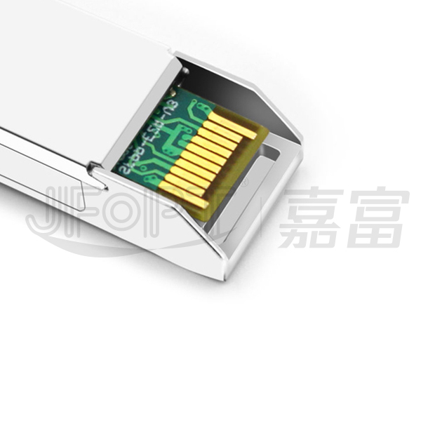
引脚定义
PIN-OUT DEFINITIONS

| Logic | Symbol | Name/Description | Note | ||||||
| 1 | - | VeeT | Module transmitter ground | Note1 | |||||
| 2 | LVTTL-O | TX_fault | Module transmitter fault | Note2 | |||||
| 3 | LVTTL-I | TX_disable | Transmitter disable;Turnsofftrans mitterlaseroutput | Note3 | |||||
| 4 | LVTTL-I/O | SDA | 2-Wire serial interface data line(Same as MOD-DEF2 asdefinedin the INF-8074i) | Note4 | |||||
| 5 | LVTTL-I/O | SCL | 2-Wire serial interface clock(Same as MOD-DEF1 as defined intheINF-8074i) | Note4 | |||||
| 6 | MOD-ABS | Module absent, connected to VeeT or VeeR in the module | Note5 | ||||||
| 7 | LVTTL-I | RS0 | Rate select 0 | - | |||||
| 8 | LVTTL-O | RX_LOS | Receiver Loss of Signal indication (In FC designated as RX_LOS, in SONET designated as LOS, and in ethernet designated at signal detect) | Note2 | |||||
| 9 | LVTTL-I | RS1 | Rate select 1 | - | |||||
| 10 | - | VeeR | Module receiver ground | Note1 | |||||
| 11 | - | VeeR | Module receiver ground | Note1 | |||||
| 12 | CML-O | RD- | Receiver inverted data output | - | |||||
| 13 | CML-O | RD+ | Receiver non inverted data output | - | |||||
| 14 | - | VccR |
Module receiver ground
|
Note1 | |||||
| 15 | - | VeeR | Module receiver 3.3 V supply | - | |||||
| 16 | - | VccT | Module transmitter 3.3 V supply | Note1 | |||||
| 17 | - | VeeT | Module transmitter ground | - | |||||
| 18 | CML- I | TD+ | Transmitter non-inverted data input | - | |||||
| 19 | CML- I | TD- | Transmitter inverted data input | - | |||||
| 20 | - | VeeT | Module yransmitter ground | Note1 | |||||
Notes:
[1]The module signal ground pins, VeeR and VeeT, shall be isolated from the module case.
[2]This pin is an open collector/drain output pin and shall be pulled up with 4.7k-10kohms to Host_Vcc on the host board. Pull ups can be connected to multiple power supplies, however the host board design shall ensure that no module pin has voltage exceeding module VccT/R + 0.5 V.
[3]This pin is an open collector/drain input pin and shall be pulled up with 4.7k-10kohms to VccT in the module.
[4]See SFF-8431 4.2 2-wire Electrical Specifications.
[5]This pin shall be pulled up with 4.7k-10kohms to Host_Vcc on the host board.
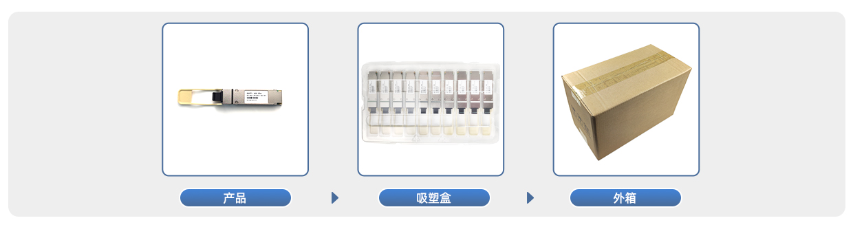
产品包装
PRODUCT PACKAGING
产品认证
PRODUCT CERTIFICATION

质量优势
QUALITY ADVANTAGE
兼容品牌
COMPATIBLE BRANDS


 Wendy
Wendy Sophie
 Jeanne


