


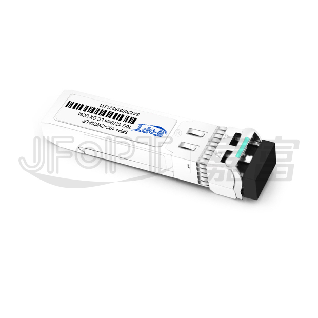
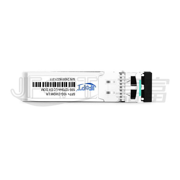

| 产品型号 | JFTSM-SFP+10-CW1216-LR-LCD | 工厂品牌 | JFOPT嘉富 |
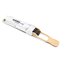
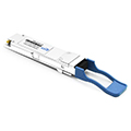
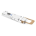
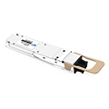
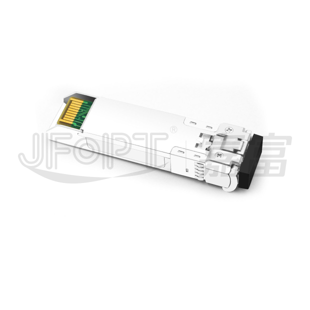
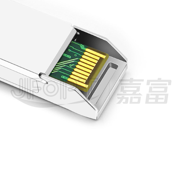
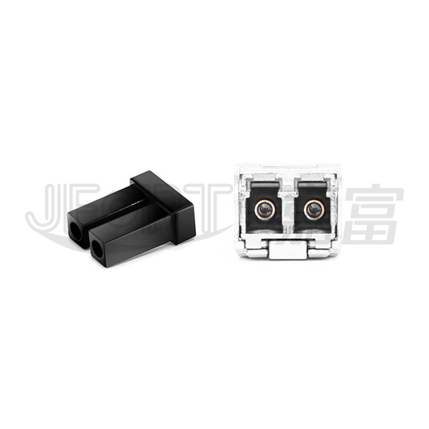
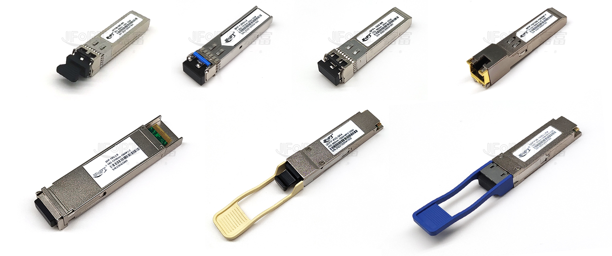
| 封装形式 | SFP+ | 光口类型 | LC Duplex |
| 最高总速率 | 11.3Gbps | 每通道速率 | 10.31Gbps |
| 功率预算 | >10dB,>14dB | ||
| 工作波长 | 1270nm to 1610nm | 工作电压 | 3.3V |
| 光纤型号 | SMF | 纤芯尺寸 | 9/125 |
| 发射器类型 | CWDM DFB | 接收器类型 | IDP |
| 发射功率 | -1~4dBm | 接收灵敏度 | -15dBm |
| 数字诊断 | YES | 接收过载 | 0.5dBm |
| 功耗 | <1W | 支持协议 | SFP+ MSA
SFF-8431
SFF-8472
|
| 工作温度(商业级) | 0℃~+70℃ | 储存温度(商业级) | -40℃~+85℃ |
| 工作温度(扩展级) | -20℃~+75℃ | 储存温度(扩展级) | -40℃~+85℃ |
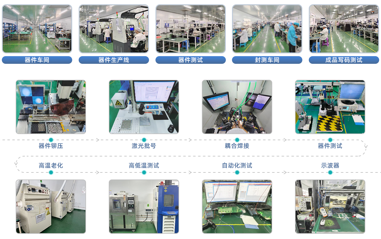
JFOPT嘉富持续投入光模块生产领域,产品覆盖1*9、SFP、10G、25G、100G、200G、400G、800G GPON/EPON/XG/XGSPON OLT等全系列光模块。同时为下游同行提供TOSA、ROSA、BOSA等光器件半成品解决方案。JFOPT嘉富生产线具备日产量一万只光模块、两万只光器件的能力。此外,JFOPT嘉富光模块拥有业界领先的耐高温、抗干扰特性,广泛应用于计算中心、运营商、交通安防、电力设施等行业领域。
JFOPT SFP+ 10G CWDM (1270-1610nm) LR LC DX系列光模块专为10G以太网(10GBASE-LR/LW)等光纤通信应用设计,完全符合SFP+多源协议(MSA) SFF-8431规范。该模块支持单模光纤CWDM波长传输,提供1270nm至1610nm范围内多个中心波长选项,波长间隔为20nm。模块采用SFP+连接器实现热插拔功能,仅需单路3.3V电源供电。关键控制特性包括:通过LVTTL逻辑高电平输入TX_DIS禁用光输出,RX_LOS指示接收光信号丢失状态,并支持基于SFF-8472标准的双线串行接口数字诊断监控。
| Up to 11.3Gb/s bit rate | Hot-pluggable SFP+ footprint | ||||||||
| 18-Wavelength CWDM DFB transmitter from 1270nm to 1610nm, with step 20nm | 10dB/14dB power budget at least | ||||||||
| Duplex LC connector | Power dissipation < 1.2W | ||||||||
| Case operation temperature range: Standard: -5°C to 70°C Extended: -20°C to 75°C |
Build-in digital diagnostic functions |
| 10GBASE-LR/LW/ER/EW 10G ethernet | 10GBASE-ER at 10.31Gbps | ||||||||
| 10GBASE-LW/EW at 9.95Gbps | OBSAI rates 6.144 Gb/s, 3.072 Gb/s, 1.536 Gb/s, 0.768Gb/s | ||||||||
| CPRI Rates 10.138Gb/s, 9.830 Gb/s,7.373Gb/s, 6.144 Gb/s,4.915 Gb/s, 2.458 Gb/s, 1.229 Gb/s, 0.614Gb/s | Other optical links |

| Part No. | Version | Data Rate | Laser | Fiber | Power Budget | Temp. | Interface | ||
| JFTSM-SFP+10-CW1216-LR-LCD-10X | Standard | Up to 11.3Gb/s | CWDM DFB | SMF | >10dB | -5°C to 70°C | LC | ||
| Extended | -20°C to 75°C | ||||||||
| JFTSM-SFP+10-CW1216-LR-LCD-14X | Standard | 0.614Gbps to 11.3Gbps | >14dB | -5~70°C | |||||
| *Note: X refers to CWDM Wavelength range 1270nm to 1610nm, X=A~R, denotes 1270nm to 1610nm. | |||||||||
| Band | Nomenclature | Wavelength(nm) | |||||||
| Min. | Typ. | Max. | |||||||
| O-band Original | A | 1264 | 1270 | 1277.5 | |||||
| B | 1284 | 1290 | 1297.5 | ||||||
| C | 1304 | 1310 | 1317.5 | ||||||
| D | 1324 | 1330 | 1337.5 | ||||||
| E | 1344 | 1350 | 1357.5 | ||||||
| E-band Extended | F | 1364 | 1370 | 1377.5 | |||||
| G | 1384 | 1390 | 1397.5 | ||||||
| H | 1404 | 1410 | 1417.5 | ||||||
| I | 1424 | 1430 | 1437.5 | ||||||
| J | 1444 | 1450 | 1457.5 | ||||||
| S-band Short Wavelength | K | 1464 | 1470 | 1477.5 | |||||
| L | 1484 | 1490 | 1497.5 | ||||||
| M | 1504 | 1510 | 1517.5 | ||||||
| N | 1524 | 1530 | 1537.5 | ||||||
| C-band Conventional | O | 1544 | 1550 | 1557.5 | |||||
| L-band Long Wavelength | P | 1564 | 1570 | 1577.5 | |||||
| Q | 1584 | 1590 | 1597.5 | ||||||
| R | 1604 | 1610 | 1617.5 | ||||||
| CWDM*: 18 Wavelengths from 1270nm to 1610nm, each step 20nm. |
|||||||||
| Parameter | Symbol | Min. | Typical | Max. | Unit | ||||
| Maximum supply voltage | Vcc | -0.5 | - | 4.0 | V | ||||
| Storage temperature | Ts | -40 | - | 85 | °C | ||||
| Parameter | Symbol | Min. | Typical | Max. | Unit | ||||
| Operating case temperature range | Tc | -5 | - | +70 | ℃ | ||||
| Supply voltage | Vcc | 3.13 | 3.3 | 3.45 | V | ||||
| Supply current | Icc | - | - | 350 | mA | ||||
| Data rate | - | 0.614 | - | 11.3 | Gbps | ||||
| Parameter | Symbol | Min. | Typ. | Max. | Unit | Notes | |||
Transmitter |
|||||||||
| CML inputs(Differential) | Vin | 150 | - | 1200 | mVpp | 1 | |||
| Input impedance (Differential) | Zin | 85 | 100 | 115 | ohm | - | |||
| Tx_DISABLE input voltage - high | - | 2 | - | Vcc+0.3 | V | - | |||
| Tx_DISABLE input voltage -low | - | 0 | - | 0.8 | V | - | |||
| Tx_FAULT output voltage - high | - | 2 | - | Vcc+0.3 | V | - | |||
| Tx_FAULT output voltage - low | - | 0 | - | 0.8 | V | - | |||
Receiver |
|||||||||
| CML outputs (Differential) | Vout | 350 | - | 700 | mVp-p | 1 | |||
| Output impedance (Differential) | Zout | 85 | 100 | 115 | ohm | - | |||
| Rx_LOS output voltage - high | - | 2 | - | Vcc+0.3 | V | - | |||
| Rx_LOS output voltage - low | - | 0 | - | 0.8 | V | - | |||
| MOD_DEF ( 0:2 ) | VoH | 2.5 | - | - | V | 2 | |||
| VoL | 0 | - | 0.5 | V | |||||
*Notes: 1. After internal AC coupling. 2. Reference the SFF-8472 MSA. |
|||||||||
| Parameter | Symbol | Unit | Note | JFTSM-SFP+10-CW1216-LR-LCD-10X | JFTSM-SFP+10-CW1216-LR-LCD-14X | |||||
| Min. | Typical | Max. | Min. | Typical | Max. | |||||
Transmitter |
||||||||||
| Output opt. pwr: 9/125 SMF | Pout | dBm | 1 | -5 | - | 0 | -1 | - | 4 | |
| Optical extinction ratio | ER | dB | - | 3.5 | - | - | 3.5 | - | - | |
| Optical wavelength | λ | nm | 2 | λc–6 | λc | λc+7.5 | λc–6 | λc | λc+7.5 | |
| -20dB spectrum width | Δλ | nm | - | - | - | 1 | - | - | 1 | |
| Side mode suppression ratio | SMSR | dB | - | 30 | - | - | 30 | - | - | |
| Transmitterand dispersion penalty | TDP | dB | - | - | - | 2 | - | - | 2 | |
| Average launch power of OFF transmitter | POFF | dBm | - | - | - | -30 | - | - | -30 | |
Receiver |
||||||||||
| Receiver sensitivity @ 10.7Gb/s | Pmin | dBm | 3 | - | - | -15 | - | - | -15 | |
| Maximum input power | Pmax | dBm | - | +0.5 | - | - | +0.5 | - | - | |
| Optical center wavelength | λ | nm | - | 1260 | - | 1620 | 1260 | - | 1620 | |
| Receiver reflectance | Rrf | dB | - | - | - | -27 | - | - | -27 | |
| LOS de-assert | LOSD | dBm | - | - | - | -16 | - | - | -16 | |
| LOS assert | LOSA | dBm | - | -28 | - | - | -28 | - | - | |
| LOS hysteresis | - | dB | - | 1 | - | - | 1 | - | - | |
*Notes: 1. Output power is coupled into a 9/125μm SMF. 2. ITU-T G.694.2 CWDM wavelength from 1270nm to 1610nm, each step 20nm. 3. Average received power; BER less than 1E-12 and PRBS 231-1 test pattern. |
||||||||||
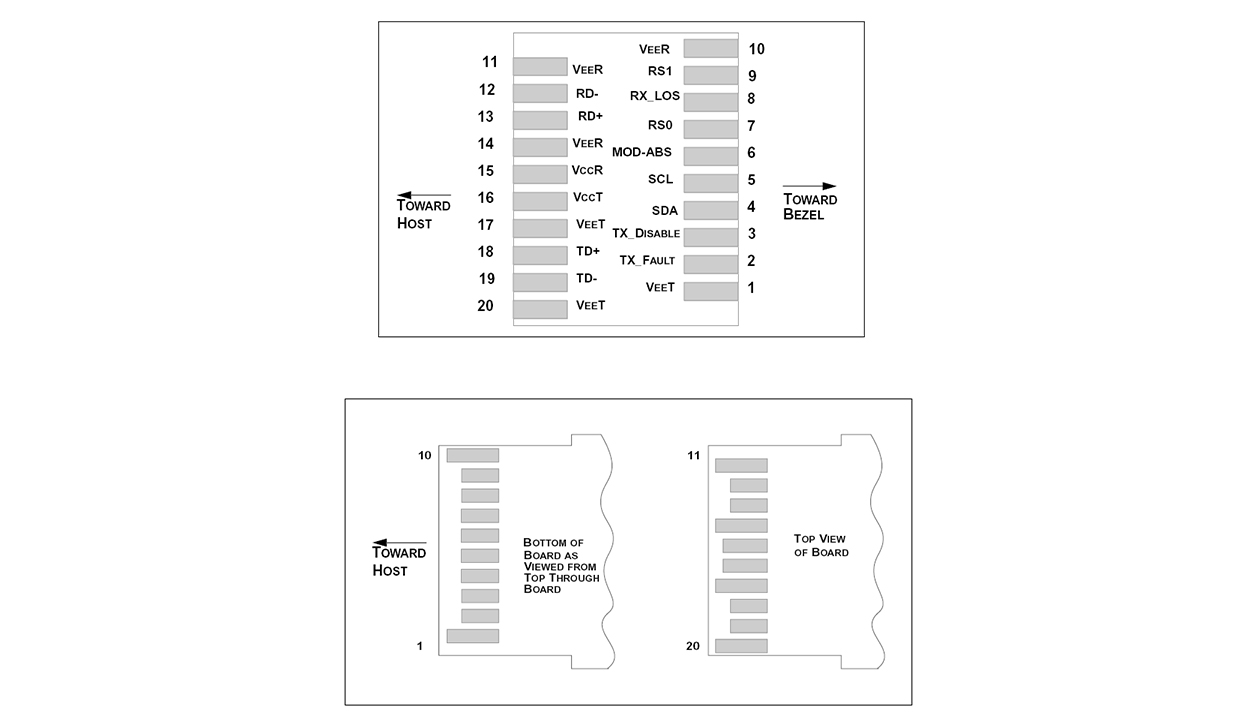
| Pin Num. | Name | Function | Plug Seq. | Notes | |||||
| 1 | VeeT | Transmitter ground | 1 | Note 5 | |||||
| 2 | TX fault | Transmitter fault indication | 3 | Note 1 | |||||
| 3 | TX disable | Transmitter disable | 3 | Note 2, module disables on high or open | |||||
| 4 | SDA | Module definition 2 | 3 | Data line for serial ID | |||||
| 5 | SCL | Module definition 1 | 3 | Clock line for serial ID. | |||||
| 6 | MOD_ABS | Module definition 0 | 3 | Note 3 | |||||
| 7 | RS0 | RX rate select(LVTTL). | 3 | No function implement.. | |||||
| 8 | LOS | Loss of signal | 3 | Note 4 | |||||
| 9 | RS1 | TX rate select(LVTTL). | 1 | No function implement.. | |||||
| 10 | VeeR | Receiver ground | 1 | Note 5 | |||||
| 11 | VeeR | Receiver ground | 1 | Note 5 | |||||
| 12 | RD- | Inv. received data out |
3
|
Note 6 | |||||
| 13 | RD+ | Received data out | 3 | Note 6 | |||||
| 14 | VeeR | Receiver ground | 1 | Note 5 | |||||
| 15 | VccR | Receiver power | 2 | 3.3V ± 5%, Note 7 | |||||
| 16 | VccT | Transmitter power | 2 | 3.3V ± 5%, Note 7 | |||||
| 17 | VeeT | Transmitter ground | 1 | Note 5 | |||||
| 18 | TD+ | Transmit data in | 3 | Note 8 | |||||
| 19 | TD- | Inv. transmit data in | 3 | Note 8 | |||||
| 20 | VeeT | Transmitter ground | 1 | Note 5 | |||||
Notes:
1) . TX Fault is an open collector/drain output, which should be pulled up with a 4.7K - 10KΩ resistor on the host board. Pull up voltage between 2.0V and VccT, R+0.3V. When high,output indicates a laser fault of some kind. Low indicates normal operation. In the low state, the output will be pulled to < 0.8V
2) . TX disable is an input that is used to shut down the transmitter optical output. It is pulled up within the module with a 4.7-10KΩ resistor. Its states are: Low (0 - 0.8V): Transmitter on(>0.8, < 2.0V): Undefined High (2.0 - 3.465V):Transmitter Disabled Open: Transmitter Disabled
3)Module absent, connected to VEET or VEER in the module
4) LOS (Loss of Signal) is an open collector/drain output, which should be pulled up with a 4.7K–10KΩ resistor. Pull up voltage between 2.0V and VccT, R+0.3V. When high, this output indicates the received optical power is below the worst-case receiver sensitivity (as defined by the standard in use). Low indicates normal operation. In the low state, the output will be pulled to < 0.8V.
5) VeeR and VeeT may be internally connected within the SFP+ module.
6) RD-/+: These are the differential receiver outputs. They are AC coupled 100Ω differential lines which should be terminated with100Ω(differential) at the user SERDES. The AC coupling is done inside the module and is thus not required on the host board.
7) VccR and VccT are the receiver and transmitter power supplies. They are defined as 3.3V ±5% at the SFP+ connector pin. Maximum supply current is 300mA. Inductors with DC resistance of less than 1 ohm should be used in order to maintain the required voltage at the SFP+ input pin with 3.3V supply voltage. When the recommended supply-filtering network is used, hot plugging of the SFP+ transceiver module will result in an inrush current of no more than 30mA greater than the steady state value. VccR and VccT may be internall connected within the SFP+ transceiver module
8) . TD-/+: These are the differential transmitter inputs. They are AC-coupled, differential lines with 100 differential termination inside the module. The AC coupling is done inside the module and is thus not required on the host board.


 Wendy
Wendy Sophie
 Jeanne


